


Designing Internet of Things (IoT) devices requires a deep understanding of how signals interact over time. Unlike high-level software development, embedded hardware design operates on strict temporal boundaries. A timing diagram serves as the visual language engineers use to communicate these boundaries clearly. This guide explores the practical application of timing diagrams within the context of IoT device architecture, focusing on signal integrity, protocol handshakes, and power management sequences.
When building connected systems, the margin for error is often measured in nanoseconds. Understanding the exact sequence of electrical events prevents data corruption and ensures reliable operation in the field. This document breaks down the essential components of timing analysis without relying on specific commercial tools, focusing instead on the underlying principles that govern device behavior.
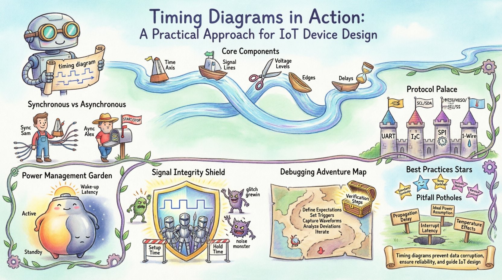
Understanding the Core Components of Timing Diagrams ⏱️
A timing diagram represents the relationship between different signals within a system. It maps out changes in voltage levels against a timeline. In IoT contexts, these signals often represent communication lines, clock pulses, or power states. To read and create these diagrams effectively, one must understand the fundamental elements that make them up.
- Time Axis: Usually runs horizontally across the bottom. It can be linear or logarithmic depending on the events being observed.
- Signal Lines: Vertical lines representing specific wires or logic nets. Each line corresponds to a physical connection or a logical state.
- Voltage Levels: Represented as high (logic 1) or low (logic 0) states. Some signals may use intermediate voltage levels for analog data.
- Edges: Transitions from low to high (rising edge) or high to low (falling edge). These edges often trigger events in the receiving circuitry.
- Delays: The time gap between a signal change and the reaction it causes. This is critical for understanding latency in data transmission.
When analyzing an IoT sensor node, for instance, the timing diagram helps visualize when the sensor wakes up, when the microcontroller reads the data, and when the radio transmits that packet. Without this visual map, debugging intermittent failures becomes nearly impossible.
Synchronous vs. Asynchronous Communication ⚡
One of the first decisions in IoT design involves selecting a communication protocol. The timing requirements differ significantly between synchronous and asynchronous methods. Understanding these differences is crucial for selecting the right interface for the specific application.
Synchronous Communication
In synchronous systems, data transfer relies on a shared clock signal. The sender and receiver agree on when to sample the data based on the clock pulses. This method generally offers higher data rates but requires more physical connections.
- Advantages: High throughput, precise timing control, and simpler error handling at the physical layer.
- Challenges: Requires a dedicated clock line, which increases pin count and power consumption. Skew between the clock and data lines can cause errors over long distances.
- Typical Use Cases: Memory interfacing, high-speed sensor data capture, and internal component communication.
Asynchronous Communication
Asynchronous systems do not use a shared clock. Instead, data is sent in packets with start and stop bits that define the boundaries. The receiver must detect these boundaries independently.
- Advantages: Fewer wires required, flexible baud rates, and robustness against minor clock drift.
- Challenges: Lower maximum data rates, potential for framing errors if the baud rate is mismatched, and higher overhead due to start/stop bits.
- Typical Use Cases: Serial debugging, low-power wake-up signals, and long-distance communication where clock skew is a concern.
Protocol Specifics in IoT Design 📡
Different communication protocols impose unique timing constraints. A generic understanding is insufficient; specific timing parameters must be adhered to for successful interoperability. Below are the common protocols encountered in embedded systems.
| Protocol | Lines Required | Timing Characteristic | Common Use |
|---|---|---|---|
| UART | 2 (Tx, Rx) | Baud rate dependent, start/stop bits | Debugging, GPS modules |
| I2C | 2 (SDA, SCL) | Open-drain, clock stretching allowed | Configuration registers, sensors |
| SPI | 4+ (MOSI, MISO, SCK, CS) | Clock polarity and phase defined | High-speed flash, displays |
| 1-Wire | 1 + Ground | Single bit, strict reset pulse timing | Temperature sensors, IDs |
Interfacing with I2C
The Inter-Integrated Circuit (I2C) bus is a staple in compact IoT designs. It uses two bidirectional lines: Serial Data (SDA) and Serial Clock (SCL). Both lines must be pulled up to a logic high state.
Timing analysis here focuses on the setup and hold times. Before the clock transitions, the data line must be stable. After the clock transition, the data must remain stable for a minimum duration. If these windows are violated, the receiving device may read incorrect data. Clock stretching is another feature where the slave device can hold the clock line low to slow down the master, ensuring it has enough time to process data.
Interfacing with SPI
The Serial Peripheral Interface (SPI) is faster than I2C but requires more pins. It is full-duplex, meaning data can be sent and received simultaneously. Timing diagrams for SPI must account for the Clock Polarity (CPOL) and Clock Phase (CPHA).
- CPOL: Determines if the clock is idle low or idle high.
- CPHA: Determines if data is sampled on the first or second clock edge.
Misinterpreting these settings leads to bit reversal or complete data loss. A practical approach involves drawing the expected waveform for both master and slave to verify alignment before hardware assembly.
Power Management and Timing 🔋
Energy efficiency is a primary concern in IoT. Devices often operate in sleep modes to conserve battery life. The timing diagram becomes essential when defining how the system transitions between active, standby, and deep sleep states.
Wake-Up Latency
When an external interrupt triggers a wake-up, the device does not become active instantly. There is a latency period where the power supply stabilizes and the internal oscillators lock in. This delay must be accounted for in the timing diagram to ensure that external peripherals are ready when the microcontroller begins executing code.
- Power-Up Sequence: Regulators ramp up voltage. Logic levels must reach valid thresholds before clocking starts.
- Initialization: Peripherals must initialize before the main application loop begins.
- Interrupt Handling: The interrupt service routine must execute within the allowed window before the next sleep cycle.
Deep Sleep Transitions
Entering a deep sleep state involves disabling clocks and turning off voltage regulators. The timing diagram must show the exact moment the system enters this state relative to the last data transmission. If the system shuts down too early, data packets may be incomplete. If it stays awake too long, battery life is compromised.
Designers must measure the time taken to transition out of deep sleep. Some circuits require a reset signal to be held for a specific duration after power is restored. Missing this timing requirement can result in boot failures.
Signal Integrity and Noise Considerations 📉
In real-world environments, electrical signals are rarely perfect. Noise, crosstalk, and impedance mismatches can distort waveforms. Timing diagrams help identify these issues by showing the ideal signal versus the actual measured signal.
Setup and Hold Times
These are critical constraints for any digital input. Setup time is the minimum time data must be stable before the clock edge. Hold time is the minimum time data must remain stable after the clock edge.
- Violation Consequences: If violated, the flip-flop may enter a metastable state, causing unpredictable logic levels.
- Remediation: Adjusting trace lengths, adding buffers, or slowing down the clock speed can resolve timing violations.
Glitches and Transients
Glitches are short-duration pulses that occur due to propagation delays in logic gates. In timing diagrams, these appear as spikes that deviate from the expected square wave. While often filtered out by hardware, persistent glitches can trigger false interrupts.
When designing for IoT, it is vital to consider the environment. Electromagnetic interference (EMI) from motors or other radios can induce voltage spikes. A timing diagram annotated with noise margins helps engineers design filters or shielding to protect the signal lines.
Debugging and Verification Process 🔍
Once a design is implemented, verification is necessary. This process involves comparing the theoretical timing diagram against the physical behavior of the hardware. This is often done using logic analyzers or oscilloscopes, though the principles remain the same regardless of the tool used.
Step-by-Step Verification
- Define Expectations: Create a reference timing diagram based on the datasheets of all components involved.
- Set Triggers: Configure the measurement hardware to trigger on specific events, such as a chip select going low.
- Capture Waveforms: Record the signal behavior during a typical operation cycle.
- Analyze Deviations: Look for violations in setup/hold times, incorrect pulse widths, or unexpected delays.
- Iterate: Adjust circuit parameters or code delays based on findings.
Annotating the Diagram
A static diagram is not enough. The diagram should be annotated with measured values. For example, instead of just showing a clock line, label the frequency and duty cycle. Instead of showing a data transition, label the rise and fall times. This level of detail turns a schematic representation into a troubleshooting map.
- Label Critical Paths: Highlight the paths where timing is tightest.
- Mark Voltage Thresholds: Clearly indicate the VIL and VIH levels.
- Include Time Zones: Divide the diagram into distinct phases, such as “Power On,” “Handshake,” and “Data Transfer.”
Common Pitfalls in IoT Timing Design ⚠️
Even experienced engineers encounter recurring issues related to timing. Being aware of these common pitfalls can save significant development time.
- Ignoring Propagation Delay: Assuming signals travel instantly across a PCB trace. Long traces introduce measurable delay.
- Assuming Ideal Power: Assuming voltage rails are stable immediately upon switch-on. Power supply ramp-up times must be factored into reset logic.
- Overlooking Interrupt Latency: Assuming an interrupt fires exactly when the signal arrives. There is always a delay due to context switching.
- Mismatched Baud Rates: In asynchronous communication, a slight mismatch between transmitter and receiver speeds causes framing errors over time.
- Ignoring Temperature Effects: Semiconductor timing characteristics change with temperature. Designs must function correctly across the full operating range.
Best Practices for Documentation 📝
Clear documentation ensures that the timing requirements are understood by everyone on the team, from hardware engineers to firmware developers. A timing diagram is a communication tool, not just a technical requirement.
- Use Standard Symbols: Adopt industry-standard symbols for signals, clocks, and buses to ensure universal understanding.
- Keep it Updated: As the design evolves, the timing diagram must be updated. Outdated diagrams lead to incorrect assumptions.
- Include Notes: Add text notes to explain non-obvious behaviors, such as open-drain requirements or pull-up resistor values.
- Version Control: Treat timing diagrams as critical documents. Track changes and maintain version history.
Summary of Key Takeaways 🎯
Timing diagrams are indispensable for IoT device design. They provide a clear picture of how signals interact over time, preventing data corruption and ensuring system stability. By understanding the differences between synchronous and asynchronous protocols, engineers can select the right interface for their needs. Power management timing ensures energy efficiency without sacrificing reliability. Signal integrity analysis protects against noise and interference.
Successful implementation requires rigorous verification. Comparing theoretical expectations with measured reality reveals hidden issues. Documenting these findings clearly aids in collaboration and future maintenance. Avoiding common pitfalls like ignoring propagation delay or power ramp-up times is essential for robust hardware.
Ultimately, the goal is to create devices that function reliably in diverse environments. A well-constructed timing diagram supports this goal by defining the boundaries within which the system must operate. Whether designing for industrial automation, smart home applications, or remote monitoring, the principles of timing analysis remain constant.
Focus on the fundamentals: signal levels, edge transitions, and temporal constraints. Build your designs around these truths, and you will achieve consistent performance in your IoT projects.