


Embedded systems operate in a world governed by cycles, edges, and precise intervals. Unlike general-purpose computing, where performance is often measured in throughput, embedded environments prioritize predictability. A single nanosecond of delay can cascade into system failure, data corruption, or hardware damage. At the heart of understanding and managing these constraints lies the timing diagram.
A timing diagram is not merely a drawing; it is a contract between hardware and software. It visualizes how signals interact over time, defining the acceptable windows for data transmission, state transitions, and interrupt handling. For engineers, neglecting these diagrams is akin to building a bridge without calculating load limits. This guide explores the anatomy, application, and critical necessity of timing diagrams in ensuring robust embedded software reliability.
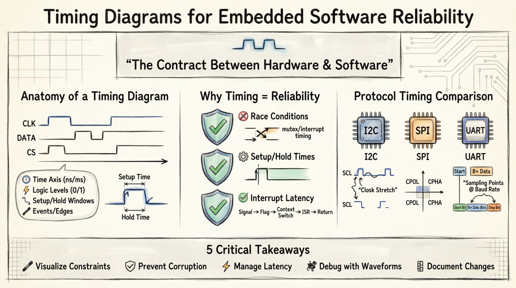
🧩 The Anatomy of a Timing Diagram
Before diving into reliability implications, one must understand the components that constitute a timing diagram. These visual representations map the logic states of signals against a time axis. They are the language used to communicate temporal requirements between system architects, hardware designers, and software developers.
- Signal Lines: Horizontal lines represent individual signals, such as clocks (CLK), data lines (SDA, SCL), or control pins (CS, RD, WR).
- Time Axis: The horizontal dimension indicates the passage of time. Units vary from nanoseconds (ns) for high-speed serial buses to milliseconds (ms) for power management sequences.
- Logic Levels: Vertical states represent binary values, typically High (1/VCC) or Low (0/GND). Transitions are shown as rising or falling edges.
- Events: Specific actions, such as a clock pulse or a data transition, are marked to show dependencies.
- Setup and Hold Times: Critical windows before and after a clock edge where data must remain stable to be read correctly.
When these elements are arranged correctly, they reveal the timing budget available for software execution. They expose bottlenecks where the processor must wait for external hardware, often referred to as bus arbitration or polling loops.
⚙️ Why Timing Diagrams Define Reliability
Reliability in embedded software is synonymous with determinism. The system must behave identically under the same conditions, every time. Timing diagrams provide the baseline for verifying this determinism. Without them, software is written in a vacuum, ignoring the physical reality of signal propagation and clock synchronization.
1. Preventing Race Conditions
A race condition occurs when the system behavior depends on the relative timing of events. In a multi-threaded or interrupt-driven environment, two tasks might attempt to access the same resource simultaneously. A timing diagram clarifies the sequence of operations.
- Scenario: An interrupt service routine (ISR) updates a variable while the main loop reads it.
- Diagram Insight: The diagram shows the ISR execution window relative to the main loop cycle.
- Resolution: Engineers can implement mutexes or disable interrupts for specific durations, ensuring the variable is not modified mid-read.
2. Managing Setup and Hold Times
Microcontrollers and peripherals have strict electrical requirements. Setup time is the minimum time a signal must be stable before a clock edge. Hold time is the minimum time it must remain stable after the edge.
If software configures a pin too quickly after a clock transition, the peripheral may latch incorrect data. Timing diagrams map these windows explicitly. They dictate how long the software must delay between setting a control line and toggling the clock. Ignoring these constraints leads to intermittent failures that are notoriously difficult to reproduce.
3. Defining Interrupt Latency
In real-time systems, the time between an event occurring and the software responding is critical. Timing diagrams illustrate the interrupt latency chain:
- Signal arrival at the pin.
- Peripheral detection and flag setting.
- CPU context switch (saving registers).
- Execution of the ISR.
- Return to the main context.
By visualizing this chain, developers can calculate the maximum latency. If the latency exceeds the time between incoming data packets, buffer overflows occur. The diagram highlights where optimization is needed, whether in the hardware configuration or the software priority levels.
📊 Protocol Analysis: I2C, SPI, and UART
Communication protocols are the backbone of embedded communication. Each has distinct timing requirements that must be respected to ensure data integrity. The following table contrasts common serial interfaces, highlighting their timing characteristics.
| Protocol | Type | Key Timing Constraint | Reliability Risk |
|---|---|---|---|
| I2C | Synchronous, Half-Duplex | Clock stretching (SCL low) time | ACK timeouts, bus hold-off |
| SPI | Synchronous, Full-Duplex | Clock polarity and phase (CPOL/CPHA) | Sample edge misalignment, data loss |
| UART | Asynchronous | Baud rate accuracy and sampling points | Framing errors, bit slip |
Deep Dive: I2C Clock Stretching
In I2C, a slave device may hold the clock line low to slow down communication. This is known as clock stretching. If the master expects the clock to return high within a specific window, but the slave takes longer, the master might time out. A timing diagram shows the low period of the SCL line. The software driver must be written to accommodate variable delays, rather than assuming a fixed clock speed.
Deep Dive: SPI Phase Alignment
SPI relies on precise clock edges to sample data. Depending on the mode (CPOL/CPHA), data is sampled on the rising or falling edge. If the software writes to the shift register too early or too late relative to the clock toggle, the received byte will be corrupted. Timing diagrams visualize the relationship between the Clock Edge and the Data Valid window.
🔍 Debugging and Signal Integrity
When a system fails, the root cause is often timing-related. Logic analyzers and oscilloscopes capture the actual waveforms, which are then compared against the expected timing diagrams. This process validates the design and identifies deviations.
1. Identifying Skew
Sky refers to the difference in arrival times of signals on parallel buses. In high-speed interfaces, if the clock arrives at the receiver before the data, setup violations occur. Timing diagrams allow engineers to measure this skew. If the skew exceeds the margin, the system becomes unstable at higher frequencies.
2. Detecting Glitches
Glitches are transient spikes that can trigger false interrupts or flip-flops. A timing diagram showing a clean transition might look perfect in simulation but reveal noise spikes in reality. By capturing the waveform, engineers can add debouncing logic in software or filter components in hardware.
3. Analyzing Power Sequencing
Embedded systems often have multiple voltage domains. Powering up a peripheral before the main logic is ready can cause latch-up or undefined states. Timing diagrams for power sequencing define the minimum delay between power rail activation and clock enable. Software drivers must enforce these delays during initialization routines.
🧱 Handling Clock Domain Crossing
Modern embedded systems often use multiple clock sources. For instance, a CPU might run at 100MHz while a communication peripheral runs at 10MHz. Transferring data between these domains creates a clock domain crossing (CDC) issue. Signals synchronized to one clock may appear metastable to the other.
A timing diagram for CDC shows the relationship between the source clock edge and the destination clock edge. To mitigate this, software must implement synchronizer circuits or handshake protocols (like Ready/Valid signals). The diagram dictates the handshake timing: the source asserts Ready, the destination samples it, and then asserts Valid. The timing between these assertions must be clear of race conditions.
🛠️ Best Practices for Implementation
To maintain reliability, engineers should integrate timing diagrams into the development lifecycle. Here are actionable practices to ensure consistency.
- Define Constraints Early: Establish timing requirements in the specification phase. Do not wait for hardware to arrive.
- Version Control Diagrams: Treat timing diagrams like code. Update them when hardware revisions change pinouts or clock speeds.
- Automated Verification: Where possible, use static analysis tools to check if code execution time fits within the timing windows defined in the diagrams.
- Document Edge Cases: Highlight scenarios like low battery voltage or temperature extremes that might slow down signal propagation.
- Validate with Hardware: Simulations are useful, but real-world signal integrity often differs. Use a logic analyzer to verify the actual timing matches the diagram.
⚡ Interrupt Priorities and Timing
In complex systems, multiple interrupts can fire simultaneously. The timing diagram of interrupt handling shows the priority hierarchy. High-priority interrupts should not be blocked by low-priority ones for extended periods.
Consider a safety-critical system monitoring a motor. If a low-priority logging task holds the CPU, the motor protection interrupt might be delayed. The timing diagram visualizes the maximum interrupt blocking time. This informs the decision on whether to use hardware priorities or software masking strategies.
🔄 DMA and Memory Access Timing
Direct Memory Access (DMA) allows peripherals to transfer data without CPU intervention. However, this introduces bus contention. When the CPU and DMA both access memory, arbitration logic determines who gets access first.
A timing diagram for DMA shows the bus request (BRQ) and bus grant (BG) signals. If the software expects data to be ready immediately after a DMA transfer, but the bus is busy with another operation, the read will fail. Understanding this bus arbitration timing prevents race conditions in data buffers.
📝 Documentation and Maintenance
Timing diagrams are living documents. As firmware evolves, the timing requirements may shift. For example, adding a new feature might increase interrupt latency, requiring a change in the communication protocol timing.
Effective documentation includes:
- Versioning: Each diagram should have a revision number linked to the firmware release.
- Reference Points: Clearly mark where the time axis starts (e.g., Power On Reset).
- Notes on Variability: Indicate if timing is worst-case or typical. Hardware tolerances mean timing is rarely exact.
Maintaining this documentation ensures that future engineers understand the constraints without needing to reverse-engineer the code. It reduces the risk of introducing regressions during updates.
🚀 Future Considerations
As embedded systems become more complex, timing analysis grows in importance. Multi-core processors introduce cache coherency timing issues. Wireless protocols add variable latency due to interference. Timing diagrams will need to evolve to represent these probabilistic elements alongside deterministic ones.
For now, the core principle remains: time is a resource that must be managed. By treating timing diagrams as a foundational artifact of the design, teams can build systems that are not just functional, but reliable under stress.
🏁 Summary of Critical Factors
To recap, the reliability of embedded software is inextricably linked to how well timing is understood and managed. Key takeaways include:
- Visualizing Constraints: Timing diagrams translate electrical specifications into software execution limits.
- Preventing Data Corruption: Setup and hold times prevent logic errors in peripherals.
- Managing Latency: Interrupt and DMA timing ensure real-time responsiveness.
- Debugging Tool: Comparing expected diagrams against captured waveforms isolates hardware and software faults.
- Documentation: Maintaining accurate diagrams preserves design intent across product lifecycles.
When engineers prioritize these temporal relationships, they reduce the likelihood of field failures. The result is a system that performs consistently, safely, and efficiently. In the intricate dance between silicon and code, the timing diagram is the sheet music that keeps everything in rhythm.