


In the complex world of embedded electronics, communication is everything. Devices do not talk with words; they speak in pulses, clock cycles, and voltage states. To understand this digital conversation, engineers rely on a specific visual language known as the timing diagram. These diagrams are the blueprints of electronic behavior, mapping out exactly when signals change state and how long those states last.
Whether you are designing a microcontroller interface or debugging a communication bus failure, understanding timing diagrams is non-negotiable. This guide provides a comprehensive look at how these diagrams function, why they are critical for embedded systems, and how to read them with precision. We will explore the fundamental components, analyze common protocols, and discuss the physical constraints that govern digital logic.
What is a Timing Diagram? ⏲️
A timing diagram is a graphical representation that shows the relationship between signals over a period of time. Unlike a circuit schematic, which shows what components are connected, a timing diagram shows when those connections are active. It is a temporal map that allows engineers to visualize data flow, synchronization, and electrical characteristics.
In embedded systems, these diagrams are essential for several reasons:
- Protocol Verification: They confirm that a device adheres to the electrical standards required by a specific communication interface.
- Debugging: When data is lost or corrupted, the timing diagram reveals if a signal arrived too early or too late.
- Design Validation: They help verify that setup and hold times are met before committing to hardware fabrication.
At its core, a timing diagram plots time along the horizontal axis and signal states along the vertical axis. This simple structure allows for the analysis of complex interactions between multiple lines of data.
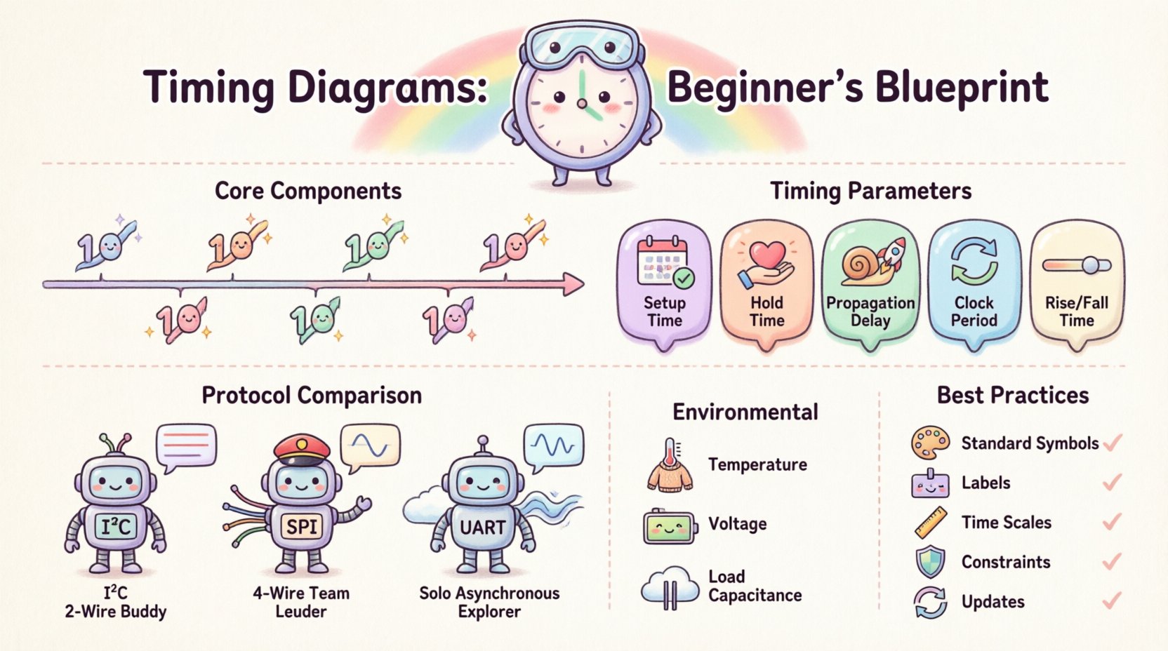
Core Components of a Timing Diagram 📊
To read a timing diagram effectively, one must understand the symbols and conventions used. While variations exist depending on the industry, the fundamental building blocks remain consistent across most digital logic documentation.
1. The Time Axis
The horizontal line represents the passage of time. It usually flows from left to right. This axis can be linear or logarithmic, though linear is standard for most embedded applications. Markers on this axis indicate specific time intervals, such as nanoseconds (ns) or microseconds (μs). Understanding the scale is crucial; a signal edge that looks instantaneous on a millisecond scale might represent a critical setup violation on a nanosecond scale.
2. Signal Lines
Vertical lines represent individual signals, such as a clock line, data lines, or control signals like chip select. Each line corresponds to a physical pin on a chip or a wire on a PCB. Signals are typically labeled with their function (e.g., SCK, MISO, CS).
3. Logic Levels
Signals in digital systems exist in discrete states. The most common representation is binary:
- High (Logic 1): Often represented by the upper voltage rail.
- Low (Logic 0): Often represented by the ground rail.
Some diagrams may also show High-Z (High Impedance), indicating that a line is electrically disconnected or floating, which is common in open-drain configurations.
4. Edges and Transitions
Edges indicate the moment a signal changes state. These are critical for synchronization:
- Rising Edge: A transition from Low to High.
- Falling Edge: A transition from High to Low.
Many protocols trigger data transfer on a specific edge of a clock signal. Misinterpreting which edge is active can lead to complete system failure.
Common Timing Parameters ⚙️
Embedded systems operate under strict physical constraints. Components do not switch states instantaneously; there is always a delay. Timing diagrams capture these delays through specific parameters. Understanding these metrics is vital for ensuring system stability.
| Parameter | Description | Why It Matters |
|---|---|---|
| Setup Time | The minimum time data must be stable before the clock edge. | Violating this causes the receiving device to read incorrect data. |
| Hold Time | The minimum time data must remain stable after the clock edge. | Violating this can cause metastability or data corruption. |
| Propagation Delay | The time taken for a signal to travel from input to output. | Affects the maximum speed the system can operate. |
| Clock Period | The duration of one complete cycle of the clock signal. | Defines the maximum operating frequency of the bus. |
| Rise/Fall Time | The time taken for a signal to transition between logic levels. | Slow transitions can cause errors or excessive power consumption. |
These parameters are not arbitrary; they are defined by the manufacturer of the silicon. When designing a system, you must ensure your external circuitry can meet these requirements. If the timing constraints are not met, the system may work at low temperatures but fail at high temperatures, or vice versa.
Interpreting Real-World Protocols 📡
While generic timing diagrams explain the theory, embedded systems rely on specific protocols. Each protocol has its own timing requirements. Below, we examine the timing characteristics of three common interfaces.
1. I2C (Inter-Integrated Circuit)
I2C is a synchronous serial communication protocol that uses two lines: SDA (data) and SCL (clock). It is widely used for connecting low-speed peripherals like sensors.
- Start Condition: The SDA line transitions from High to Low while the SCL line is High. This signals the beginning of a transmission.
- Stop Condition: The SDA line transitions from Low to High while the SCL line is High. This signals the end of transmission.
- Data Validity: Data on the SDA line must remain stable while SCL is High. Changes only occur when SCL is Low.
- Open-Drain: Both lines are typically pulled up to a voltage rail. Devices pull the line Low to transmit a 0.
2. SPI (Serial Peripheral Interface)
SPI is a faster synchronous protocol using four lines: MOSI (Master Out Slave In), MISO (Master In Slave Out), SCK (Clock), and SS (Slave Select).
- Master Control: The master device controls the clock frequency and the chip select lines.
- Clock Polarity: The diagram must indicate if the clock idles High (CPOL=1) or Low (CPOL=0).
- Clock Phase: Data is sampled on the first or second edge of the clock cycle (CPHA).
- Chip Select: The SS line must be active (usually Low) for the duration of the entire transaction.
3. UART (Universal Asynchronous Receiver-Transmitter)
UART is an asynchronous protocol, meaning it does not share a clock line. Timing relies on both devices agreeing on a baud rate.
- Idle State: The line sits High.
- Start Bit: A transition to Low indicates the start of a byte.
- Data Bits: Follow the start bit, usually LSB first.
- Stop Bit: Returns the line to High to mark the end of the byte.
In asynchronous systems, timing diagrams must account for jitter. If the receiver samples the data too early or too late relative to the transmitter’s baud rate, errors will occur.
Reading and Creating Timing Diagrams 📝
Creating a timing diagram is a systematic process. It requires attention to detail and a clear understanding of the system’s operational flow. Follow these steps to ensure accuracy.
Step 1: Identify the Signals
List all relevant signals involved in the interaction. This includes data lines, control lines, and clock signals. Do not omit auxiliary signals like interrupts or resets, as they can affect timing.
Step 2: Establish the Timeline
Decide on the time scale. For high-speed interfaces, nanoseconds are necessary. For slower control signals, milliseconds may suffice. Mark the key events, such as a reset pulse or a data transfer start.
Step 3: Map the Edges
Draw the transitions. Ensure that the rising and falling edges align correctly with the clock cycles. Check that setup and hold times are visually represented clearly.
Step 4: Annotate Conditions
Add notes to explain specific states. For example, indicate if a line is in High-Z mode or if a specific voltage threshold is required for a logic transition.
Step 5: Review and Validate
Compare your diagram against the datasheets of the components. Verify that the timing parameters meet the manufacturer’s specifications. This step is critical before moving to hardware implementation.
Common Pitfalls and Troubleshooting 🚫
Even with careful planning, timing issues can arise. These problems often manifest as intermittent failures that are difficult to reproduce. Understanding common pitfalls helps in diagnosing these issues.
1. Metastability
Metastability occurs when a signal violates setup or hold time requirements. The receiving flip-flop enters an indeterminate state where the output voltage is neither High nor Low. This can propagate through the system, causing unpredictable behavior. To mitigate this, designers often use synchronizers to allow extra time for the signal to stabilize.
2. Clock Skew
Clock skew happens when the clock signal arrives at different components at different times. This is often caused by trace length differences on a PCB. If the skew exceeds the timing margin, data may be sampled incorrectly. Routing clock lines with matched lengths helps reduce this risk.
3. Signal Integrity and Glitches
Electrical noise can cause false transitions, known as glitches. These are short pulses that do not represent valid data. They can be caused by crosstalk or ground bounce. Filtering these signals or shielding sensitive lines is necessary for robust designs.
4. Asynchronous Domain Crossing
Transferring data between two different clock domains is risky. If the clocks are not synchronized, timing diagrams may show valid data on one side but invalid data on the other. Special handshaking protocols are required to manage this transition safely.
Best Practices for Documentation 📋
Clear documentation ensures that other engineers can understand and maintain the system. A well-crafted timing diagram is a vital part of this documentation.
- Use Standard Symbols: Stick to industry-standard representations for edges and states to avoid confusion.
- Label Everything: Ensure every line has a clear label corresponding to the pinout.
- Include Time Scales: Always indicate the time unit for the horizontal axis.
- Highlight Constraints: Use brackets or shading to show critical timing windows like setup and hold periods.
- Keep it Updated: As hardware changes, the timing diagrams must be updated to reflect the new reality.
The Impact of Environmental Factors 🌡️
Timing is not static. It is influenced by the physical environment in which the device operates. Engineers must consider these variables when creating timing diagrams for production hardware.
Temperature: Semiconductor performance degrades at extreme temperatures. At high temperatures, propagation delays increase, which can cause setup time violations. Conversely, at very low temperatures, leakage currents decrease, which might alter rise times.
Voltage: Supply voltage fluctuations affect switching speeds. Lower voltage generally results in slower switching, increasing propagation delay. Timing diagrams should ideally account for the worst-case voltage scenarios defined by the power supply specifications.
Load Capacitance: The physical capacitance of the PCB traces and connected devices affects the rise and fall times of signals. High capacitance slows down transitions. This is particularly relevant for high-speed buses where signal integrity is paramount.
Conclusion on Timing Accuracy 🏁
Mastering the art of reading and creating timing diagrams is a fundamental skill for anyone working with embedded systems. These visual tools bridge the gap between abstract logic and physical reality. They allow engineers to predict how a circuit will behave before a single chip is soldered.
By understanding the core components, parameters, and protocols, you can design systems that are robust and reliable. Attention to setup and hold times, clock skew, and environmental factors ensures that your device functions correctly under real-world conditions. As technology advances and speeds increase, the importance of precise timing analysis will only grow. Prioritize clarity in your documentation and rigor in your analysis to build systems that stand the test of time.