


Understanding the flow of signals over time is critical for any engineer working with digital systems, hardware interfaces, or high-performance software. When data moves too fast, too slow, or at the wrong moment, bugs appear that are notoriously difficult to track down. These are known as timing-related bugs. A timing diagram provides a visual map of these events, allowing engineers to see exactly when signals change state relative to a clock or another signal. This guide explores how to use timing diagrams effectively to identify, analyze, and resolve timing issues in your projects.
📐 What is a Timing Diagram?
A timing diagram is a graphical representation of how signals change state over time. It is not merely a waveform viewer; it is a structured document that aligns multiple signals on a common time axis. In the context of debugging, it serves as a forensic tool. Just as a detective reviews a timeline of events to solve a crime, an engineer reviews a timing diagram to find the moment a signal deviated from its expected behavior.
- Horizontal Axis: Represents time. It can be linear or logarithmic depending on the zoom level.
- Vertical Axis: Represents individual signals or nets. Each line corresponds to a specific wire, register, or logical state.
- States: Signals are typically binary (High/Low, 1/0) but can represent multi-bit values or voltage levels.
- Transitions: The movement from one state to another is marked by rising or falling edges.
Without a timing diagram, debugging is often a process of blind guessing. You might change a register value or add a delay, hoping it fixes the issue. With a timing diagram, you have concrete evidence of where the synchronization failed. This visual evidence removes ambiguity from the debugging process.
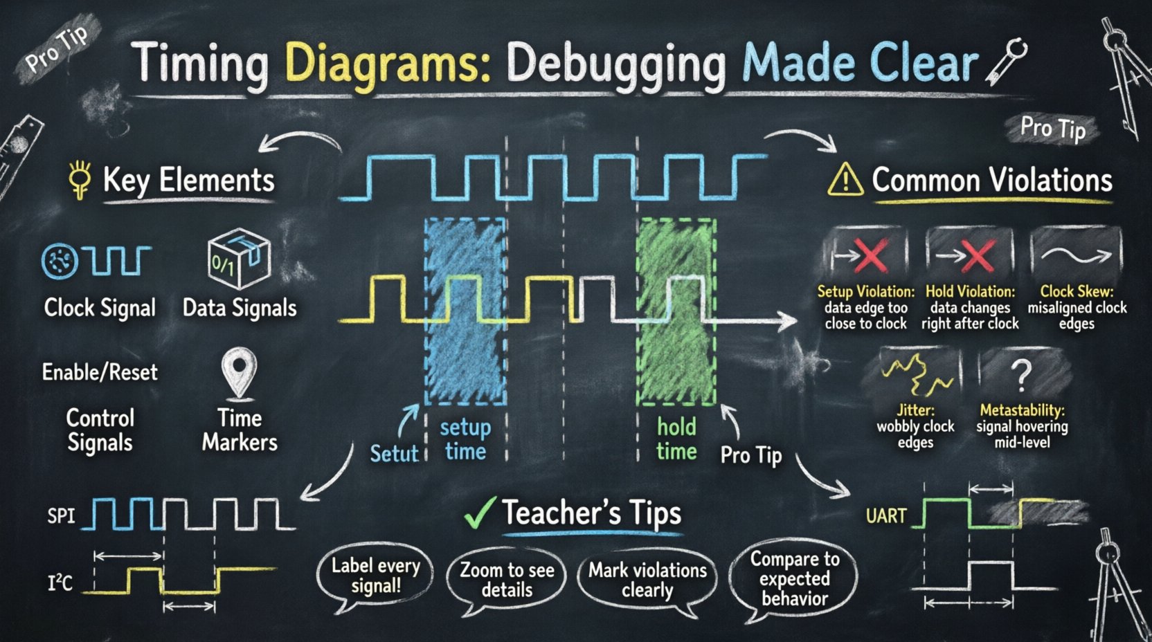
🔍 Key Elements of a Timing Diagram
To interpret these diagrams correctly, you must understand the fundamental components that make them up. Every signal trace contains specific characteristics that define its behavior.
1. Clock Signals
The clock is the heartbeat of synchronous systems. It dictates when data should be sampled or updated. A clock signal is usually a square wave with a specific frequency. In a diagram, it is often the first signal listed at the top. You must identify the active edge—rising or falling—which triggers the data capture.
2. Data Signals
These are the signals carrying actual information. They must remain stable during specific windows relative to the clock edge. If a data signal changes too close to the clock edge, the system might read the wrong value.
3. Control Signals
Signals like Enable, Chip Select, or Reset control the flow of data. They often gate the clock or inhibit updates. In debugging, these are the first places to check when a device is not responding as expected.
4. Time Markers
Specific points on the timeline are labeled to indicate setup time, hold time, or propagation delay. These markers help quantify whether a violation has occurred.
⚙️ Why Timing Diagrams are Critical for Debugging
Timing bugs are often non-deterministic. They might happen only when the system is hot, or only when a specific sequence of events occurs rapidly. This makes them hard to reproduce in a lab. A timing diagram captures the exact sequence, preserving the state of the system at a specific moment.
Here is why this tool is indispensable:
- Visualizing Race Conditions: When two signals compete to drive a bus, a timing diagram shows which one arrived first.
- Identifying Glitches: Short, unintended pulses can trigger logic incorrectly. These are often invisible in logical analysis but clear in a timing view.
- Verifying Protocol Compliance: Standards like I2C or SPI have strict timing requirements. A diagram proves compliance or highlights the deviation.
- Understanding Latency: It helps calculate the delay between an input event and a system response.
⚠️ Common Timing Violations and Solutions
Certain timing issues occur frequently in digital design. Recognizing the signature of these violations in a diagram can speed up the fix significantly.
| Violation Type | Description | Visual Signature | Common Fix |
|---|---|---|---|
| Setup Time Violation | Data changes too close before the clock edge. | Data edge is too near the clock rising edge. | Increase clock period or optimize logic path. |
| Hold Time Violation | Data changes too soon after the clock edge. | Data edge overlaps the clock rising edge. | Add delay to data path or buffer. |
| Clock Skew | Clock arrives at different destinations at different times. | Multiple clock edges are misaligned horizontally. | Improve clock distribution network. |
| Jitter | Uncertainty in the clock period. | Edges wobble or vary in position. | Use better clock source or PLL. |
| Metastability | Signal is neither high nor low for a period. | Signal hovers in an intermediate voltage level. | Use synchronizer flip-flops. |
🕰️ Deep Dive: Setup and Hold Times
Two concepts dominate timing analysis: setup time and hold time. These are the most common sources of failures in synchronous circuits.
Setup Time
Setup time is the minimum amount of time the data signal must be stable before the clock edge arrives. If the data changes within this window, the receiving flip-flop might not capture the correct value. On a timing diagram, you will see the data line transitioning too close to the clock line.
- Impact: If violated, the system might read garbage data or enter a metastable state.
- Debugging: Look for data transitions that occur too early relative to the clock edge.
Hold Time
Hold time is the minimum amount of time the data signal must remain stable after the clock edge. The flip-flop needs this time to latch the value securely. If the data changes immediately after the clock, the previous value might be overwritten prematurely.
- Impact: Similar to setup violations, this leads to incorrect data capture.
- Debugging: Look for data transitions that occur immediately following the clock edge.
📉 Skew and Jitter
Even if setup and hold times are met, other factors can degrade performance. Skew and jitter are subtle issues that require careful observation.
Clock Skew
Skew occurs when the clock signal reaches different parts of the circuit at different times. This can happen due to physical distance on a PCB or variations in routing. In a timing diagram, you will see the clock edge for Signal A arriving slightly before or after Signal B.
- Positive Skew: Clock arrives late at the destination. This helps setup time but hurts hold time.
- Negative Skew: Clock arrives early at the destination. This helps hold time but hurts setup time.
Clock Jitter
Jitter is the short-term variation of a signal with respect to its ideal position in time. It is often caused by power supply noise or interference. On a diagram, the edges might look “wobbly” or inconsistent.
- Random Jitter: Unpredictable variations, often noise-related.
- Deterministic Jitter: Patterned variations, often related to crosstalk or interference.
📡 Analyzing Protocols with Timing Diagrams
Communication protocols rely heavily on precise timing. When a device fails to communicate, a timing diagram is the first place to look.
Synchronous Protocols (SPI, I2C)
These protocols use a clock line to synchronize data transfer. The timing diagram must show the data changing on the correct clock edge (usually the falling edge for I2C).
- Check Start/Stop Bits: Ensure the start condition occurs before the first data bit.
- Check Acknowledge: Verify that the slave pulls the line low to acknowledge receipt.
Asynchronous Protocols (UART)
These protocols do not use a clock line. Timing is determined by baud rate. The diagram shows the voltage level of the data line over time.
- Check Bit Width: Ensure the pulse width matches the expected duration (e.g., 104 microseconds for 9600 baud).
- Check Parity: Verify the parity bit is present and correct.
🧩 Clock Domain Crossing (CDC)
When signals move between two clock domains (different frequencies or phases), timing becomes complex. This is known as Clock Domain Crossing. The timing diagram is vital here to ensure no data is lost.
The Problem
If a signal is sent from a fast clock domain to a slow one, the receiver might miss the pulse. If sent vice versa, the receiver might see the signal twice.
The Solution
Use synchronization techniques like multi-flop synchronizers or handshake protocols. On a timing diagram, you should see the signal being sampled multiple times across the boundary to ensure stability.
- Metastability: If the signal arrives near the clock edge in the destination domain, the output might oscillate. The diagram will show an intermediate voltage level.
- Resolution: Ensure enough time is allowed for the signal to settle before the next clock edge.
🛠️ Best Practices for Creating Timing Diagrams
To get the most out of this tool, follow these guidelines when documenting or analyzing signals.
- Label Everything: Name every signal clearly. Ambiguity leads to mistakes.
- Use Zoom Wisely: Use wide zoom for protocol flow and narrow zoom for signal integrity.
- Mark Violations: Annotate the diagram where timing constraints are breached.
- Include Context: Add notes about what triggered the event sequence.
- Export for Collaboration: Save diagrams in standard formats to share with the team.
🔄 Integrating into the Workflow
Timing analysis should not be an afterthought. It should be integrated into the design and testing phases.
- Design Phase: Define timing constraints in the specification. Create expected timing diagrams for critical paths.
- Simulation Phase: Run simulations that generate timing traces. Verify them against the expected diagrams.
- Testing Phase: Capture real-world traces using logic analyzers. Compare them to simulation data.
- Debug Phase: When a bug occurs, capture the trace immediately. Do not reset the system, as timing behavior might change.
🔎 Advanced Analysis Techniques
Beyond basic reading, there are advanced methods to extract value from timing data.
Statistical Analysis
Run multiple captures and overlay them. This reveals consistency. If the edges drift significantly between captures, you have a stability issue.
Correlation with Power
Combine timing traces with power consumption data. Sudden spikes in power might indicate a glitch or a short circuit that is also visible in the signal timing.
Automated Checking
Many tools allow you to define rules. The software can automatically flag violations of setup or hold times, reducing manual inspection time.
📝 Summary of Key Takeaways
Timing diagrams are the backbone of debugging signal integrity issues. They provide the visual evidence needed to understand why a system behaves unexpectedly. By mastering the reading of these diagrams, engineers can identify setup and hold violations, detect glitches, and ensure protocol compliance.
- Visual Clarity: Always prefer a visual timeline over raw data logs.
- Focus on Edges: The transition points are where errors usually occur.
- Know the Rules: Understand the timing requirements of the specific hardware or protocol you are using.
- Iterate: Use the diagram to test a hypothesis, implement a fix, and verify the change.
When you approach a timing bug, do not guess. Capture the data, draw the diagram, and let the timeline tell you the story. This disciplined approach saves time and ensures robust, reliable systems.