


In the world of digital electronics and software integration, time is not just a measurement; it is a constraint. Signals do not travel instantly. Logic states do not change without a trigger. When these temporal relationships are misunderstood, systems fail. This guide provides a deep dive into timing diagrams, the visual blueprints that engineers use to map the relationship between signals and time. Whether you are debugging a circuit or designing a protocol, understanding these diagrams is essential for identifying time-based errors.
What Is a Timing Diagram? 📊
A timing diagram is a graphical representation of the relationship between two or more signals over time. It functions as a timeline for logic levels. Instead of showing voltage or current directly, it shows the state of a signal (High, Low, or Floating) at specific intervals. This abstraction allows designers to focus on the sequence of events rather than the physical properties of the hardware.
Think of it as a musical score. Just as a score tells a musician when to play a note and for how long, a timing diagram tells a digital system when to change state and for how long to maintain it. Without this visual aid, coordinating multiple signals across different components would be nearly impossible.
Why They Matter 🎯
- Debugging: They reveal when data is valid and when it is not.
- Design: They help determine if a circuit meets speed requirements.
- Communication: They define the handshake protocols between devices.
- Verification: They serve as a reference for simulation and testing.
Anatomy of a Timing Diagram 🔍
To read a timing diagram effectively, you must understand its core components. Every diagram, regardless of complexity, relies on a standard structure.
The Axes
- X-Axis (Horizontal): Represents time. It flows from left to right. Time intervals can be linear or logarithmic, depending on the scale.
- Y-Axis (Vertical): Represents logic levels. Typically, the top line indicates a High state (Logic 1) and the bottom line indicates a Low state (Logic 0).
The Traces
Each horizontal line is a trace representing a specific signal. Labels are crucial. Without clear labels, a trace is meaningless. Common labels include Clock (CLK), Data (D), Enable (EN), or Address (ADDR).
Logic States
- High (H): Usually corresponds to Vcc or a positive voltage.
- Low (L): Usually corresponds to Ground or 0V.
- Undefined/Unknown (X): A state where the value is not yet determined.
- High-Z (Z): High impedance, meaning the signal is disconnected from the circuit.
Signal Transitions and Edges 🔄
Signals rarely stay static. They transition between states. Understanding these transitions is the first step in analyzing timing.
Rising and Falling Edges
- Rising Edge: The transition from Low to High. Often denoted by an upward arrow.
- Falling Edge: The transition from High to Low. Often denoted by a downward arrow.
- Edge-Triggered: Many components react only to the moment the edge occurs, not the level itself.
Active High vs. Active Low
Not all signals behave the same way when active.
- Active High: The signal performs its function when the voltage is High.
- Active Low: The signal performs its function when the voltage is Low. These are often indicated with a bar over the label (e.g.,
\overline{CS}for Chip Select).
| Feature | Active High | Active Low |
|---|---|---|
| Logic State | High (1) | Low (0) |
| Common Notation | Label Name | Label with Bar (e.g., \overline{RD}) |
| Typical Use | Data, Clock | Reset, Interrupts, Chip Select |
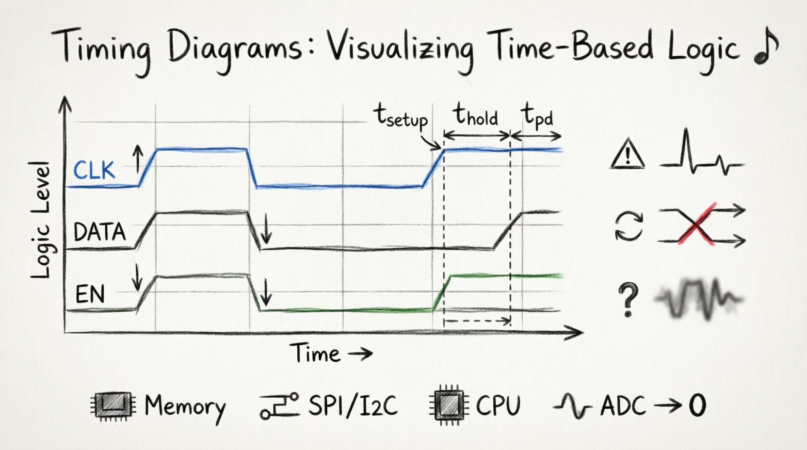
Critical Timing Parameters ⚙️
This is the core of timing analysis. Specific time measurements determine whether a system functions correctly. Missing these parameters is the primary cause of time-based errors.
Propagation Delay (tpd)
This is the time it takes for a change at the input to result in a change at the output. No signal travels instantly. Even in digital logic, there is a physical delay caused by the distance electrons must travel and the capacitance of the gates.
- Input to Output: Measured from the trigger edge to the final state change.
- Impact: Too much delay can cause a signal to arrive after the next clock cycle begins, leading to data loss.
Setup Time (tsetup)
Setup time is the minimum amount of time before a clock edge that the data signal must be stable and valid. If the data changes too close to the clock edge, the receiving device may not capture it correctly.
- Requirement: Data must be present and steady before the edge.
- Violation: Results in unpredictable data or metastability.
Hold Time (thold)
Hold time is the minimum amount of time after the clock edge that the data signal must remain stable. The capturing device needs a moment to latch the value securely.
- Requirement: Data must stay steady after the edge.
- Violation: Similar to setup violations, this causes data corruption.
| Parameter | Definition | Timing Window |
|---|---|---|
| Setup Time | Min time before clock edge | T– |
| Hold Time | Min time after clock edge | T+ |
| Propagation Delay | Time for signal to change | Tdelay |
Common Time-Based Errors 🚨
When timing diagrams are violated, specific errors occur. Recognizing these patterns is key to troubleshooting.
1. Setup and Hold Violations
These are the most frequent issues in synchronous digital design. If data arrives too early or too late relative to the clock, the flip-flop cannot latch it reliably.
- Setup Violation: Data is too slow to reach the destination before the clock arrives.
- Hold Violation: Data changes too soon after the clock arrives, overwriting the new value before it is latched.
2. Glitches
A glitch is a short, unintended pulse that appears on a signal line. These are often caused by differences in propagation delays through different logic paths. In a timing diagram, a glitch looks like a tiny spike that dips or rises briefly before settling.
- Impact: Can trigger false interrupts or corrupt data if sampled during the spike.
- Prevention: Careful logic design and the use of synchronizers.
3. Race Conditions
A race condition occurs when the system output depends on the sequence or timing of events that are otherwise unpredictable. If two signals are meant to trigger an action simultaneously, but one arrives slightly earlier, the outcome changes.
- Scenario: Two branches of logic trying to set a flag at the same time.
- Result: Unpredictable behavior that is hard to reproduce.
4. Metastability
This happens when a signal is sampled exactly during the transition period between High and Low. The output of the flip-flop does not settle to a valid 0 or 1 immediately. It hovers in an undefined state for an unpredictable amount of time.
- Causes: Clock domain crossing or asynchronous inputs.
- Mitigation: Use synchronizer chains (two or more flip-flops in series).
Reading and Analyzing a Diagram 🧐
Once you have the diagram in front of you, follow a systematic approach to analyze it.
- Identify the Clock: Find the periodic signal. This is your reference point. All timing measurements usually relate to this.
- Locate the Data: Find the signal carrying the information. Look for changes relative to the clock edges.
- Check Valid Windows: Draw vertical lines at the clock edges. Measure if the data is stable within the setup and hold windows.
- Look for Latency: Compare the time of the input event to the time of the output event. Is the delay within specification?
- Trace Dependencies: See how one signal affects another. Does Signal A need to be high before Signal B can toggle?
Real-World Applications 🌐
Timing diagrams are not just theoretical exercises. They are used in critical systems daily.
1. Memory Interfaces
When reading from RAM, the timing diagram dictates exactly when the address is sent, when the read strobe is asserted, and when the data becomes valid on the bus. Missing a single nanosecond here can cause a system crash.
2. Communication Protocols
Protocols like I2C, SPI, and UART rely entirely on timing. I2C, for example, requires the data line to be stable when the clock line is high. The timing diagram defines the bit rate and the start/stop conditions.
3. Processor Architecture
CPU pipelines depend on precise timing. Instructions must be fetched, decoded, and executed in lockstep. Timing diagrams help engineers ensure that the clock frequency does not exceed the speed of the slowest component in the pipeline.
4. Analog-to-Digital Conversion
ADCs require specific sampling windows. The timing diagram shows when the analog signal is captured and when the digital output is ready. If the sampling rate is too low, aliasing occurs.
Best Practices for Design 🛠️
Creating reliable systems requires planning the timing early. Do not treat timing as an afterthought.
- Account for Skew: Clock skew is the difference in arrival times of the clock signal at different components. Long traces cause more delay. Plan for this in your layout.
- Use Synchronizers: Always synchronize asynchronous signals using a chain of flip-flops to reduce metastability risk.
- Verify Margins: Design with margins. If a component requires 5ns of setup time, aim for 10ns to account for temperature and voltage variations.
- Document Clearly: When creating diagrams, ensure labels are clear, time scales are marked, and logic levels are defined.
Troubleshooting Checklist 🔎
When a system fails intermittently, a timing diagram is your first tool. Use this checklist to guide your investigation.
- Check Clock Stability: Is the clock signal clean? Are there jitter spikes?
- Measure Signal Levels: Are the High and Low voltages within the specification range?
- Verify Edge Alignment: Do the data edges align correctly with the clock edges?
- Inspect for Noise: Look for small spikes or ripples that might look like glitches.
- Review Load Capacitance: Are you driving too many inputs with one output? This slows down transitions.
- Check Reset Sequences: Does the system reset properly before starting operations? Improper reset timing causes state machine errors.
The Physics of Signal Integrity 📏
While timing diagrams are logical representations, they are grounded in physics. Understanding the physical constraints helps explain why the diagrams look the way they do.
Propagation Velocity
Signals travel through traces at a fraction of the speed of light. This velocity depends on the dielectric material of the PCB. A signal takes longer to travel across a long board than a short one. This physical distance is often the source of timing delays that diagrams must account for.
Capacitance and Inductance
Every wire has capacitance and inductance. These properties resist changes in voltage and current. This causes the edges of the signal to become rounded rather than sharp square waves. Slow edges can confuse logic gates that expect fast transitions.
Temperature and Voltage
Timing parameters are not constant. They change with temperature and supply voltage. A chip that works at 25°C might fail at 85°C because the internal transistors slow down. Timing diagrams often include “worst-case” scenarios to account for these environmental factors.
Advanced Concepts: Clock Domain Crossing ⚡
One of the most complex areas in timing analysis is crossing between different clock domains. This occurs when data moves from a circuit running at one frequency to a circuit running at another.
- Asynchronous Risks: If clocks are unrelated, setup and hold times cannot be guaranteed.
- Solution: Use FIFOs (First-In-First-Out buffers) or handshake protocols to manage the transfer safely.
- Visualizing: In a timing diagram, you will see two separate clock traces. The data trace must be carefully analyzed to ensure it does not violate timing relative to either clock.
Summary and Next Steps 📚
Timing diagrams are the language of synchronization in digital systems. They translate physical behavior into readable logic. By mastering the interpretation of these diagrams, you gain the ability to predict system behavior and prevent errors before they manifest.
Start by analyzing simple diagrams. Practice identifying setup and hold windows. As you gain confidence, move to complex multi-clock systems. Remember that time is a finite resource in electronics. Every nanosecond counts. Treat timing diagrams with the respect they deserve, and your designs will be more robust and reliable.
Continue to study signal integrity, clock distribution networks, and protocol specifications. These topics complement the knowledge gained here and deepen your understanding of the digital landscape.