


In the intricate world of embedded systems and Internet of Things (IoT) architecture, timing is not merely a metric; it is a fundamental constraint that dictates system stability. When multiple threads or interrupts attempt to access shared resources simultaneously, the potential for a race condition emerges. This guide provides a technical examination of how to diagnose such synchronization issues using timing diagrams. We will explore the mechanics of concurrent execution, analyze signal transitions, and identify the precise moment where logic diverges from intended behavior.
🧩 Understanding Concurrency in Embedded Systems
IoT devices often operate under strict power and processing constraints. To maximize efficiency, developers frequently implement concurrent processes. This means the central processing unit (CPU) handles multiple tasks, such as sensor polling, network transmission, and actuator control, seemingly at the same time. However, true parallelism is rare in single-core microcontrollers. Instead, rapid context switching creates the illusion of simultaneity.
- Shared Memory: Variables accessible by both an interrupt service routine (ISR) and the main loop.
- Hardware Peripherals: Registers used for UART, SPI, or I2C communication.
- State Machines: Logic that transitions based on external triggers.
When these elements interact without proper synchronization primitives, the system state becomes non-deterministic. A race condition occurs when the outcome of a process depends on the relative timing of events that are not guaranteed to occur in a specific order.
📊 The Role of Timing Diagrams in Debugging 🛠️
A timing diagram is a visual representation of signals over a defined time axis. In the context of debugging, it serves as a forensic tool. Unlike a static code review, a timing diagram captures the dynamic behavior of the hardware and software interaction. It allows engineers to see latency, jitter, and overlapping execution windows.
Key Components of a Timing Diagram
| Component | Description | Relevance to Race Conditions |
|---|---|---|
| Time Axis | Horizontal line representing duration (ns, μs, ms) | Establishes the sequence of events |
| Signal Lines | Vertical lines representing specific pins or variables | Shows high/low states or data changes |
| Transitions | Edges where signal state changes (rising/falling) | Indicates trigger points for interrupts |
| Latency Markers | Delays between trigger and response | Reveals processing bottlenecks |
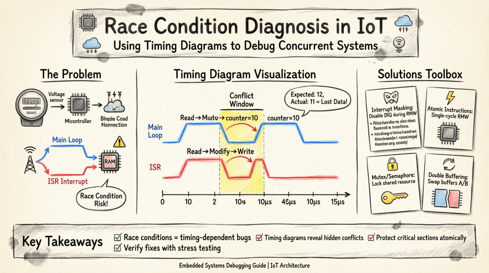
🏭 Case Study Scenario: Smart Energy Meter
Consider an IoT energy meter designed to measure voltage and current pulses. The device must log these pulses to non-volatile memory while simultaneously transmitting a summary packet to a cloud gateway via a cellular module. The system architecture involves a main application loop and a hardware interrupt triggered by a voltage threshold crossing.
System Specifications
- Microcontroller: 32-bit ARM Cortex-M4 based processor
- Shared Resource: A 4-byte counter variable in RAM
- Interrupt Source: External voltage comparator
- Main Loop Task: Periodic data aggregation and transmission
The intended logic is simple: when a voltage spike occurs, the interrupt increments the counter. The main loop reads the counter, transmits the value, and resets it to zero. Under normal load, this works. However, under high load conditions, data corruption occurs.
📈 Analyzing the Signal Flow
To diagnose the issue, we construct a timing diagram focusing on the interaction between the Interrupt Service Routine (ISR) and the Main Loop. The diagram visualizes the CPU execution flow, the signal state of the shared counter, and the status of the peripheral data bus.
Phase 1: The Read-Modify-Write Cycle
The core of the race condition lies in the Read-Modify-Write (RMW) sequence. This operation is not atomic on many architectures. It involves three distinct steps:
- Read: The CPU fetches the current value from memory.
- Modify: The CPU adds one to the register value.
- Write: The CPU stores the new value back to memory.
If an interrupt occurs between step 1 and step 3, the integrity of the data is compromised. Let us examine the timing diagram representation of this event.
Timing Diagram Visualization
| Time (μs) | Main Loop | ISR | Shared Counter Value |
|---|---|---|---|
| 0 | Read Counter (Value: 10) | Idle | 10 |
| 2 | Register holds 10 | Interrupt Triggered | 10 |
| 5 | Modify (10 + 1 = 11) | Read Counter (Value: 10) | 10 |
| 8 | Interrupt Pending | Modify (10 + 1 = 11) | 10 |
| 10 | Write (11) | Write (11) | 11 |
| 12 | Reset Counter (0) | Return to Interrupt | 0 |
| 15 | End of Cycle | Return to Main Loop | 0 |
Notice the discrepancy in the final value. Both the Main Loop and the ISR read the value 10. Both add one, resulting in 11. The Main Loop writes 11. The ISR overwrites this with 11. The net result is a count of 11, when it should be 12. The pulse detected by the ISR was effectively lost because the Main Loop was in the middle of processing the previous count.
🔍 Identifying the Conflict Window
The timing diagram makes the conflict window visible. This is the interval between the Main Loop reading the variable and writing the new value. In this specific architecture, the cycle takes approximately 8 microseconds. The interrupt latency must be shorter than this window for the race condition to occur.
Factors Influencing the Window
- Clock Speed: Higher frequencies reduce the physical time of the RMW cycle.
- Memory Latency: Wait states in SRAM or Flash can extend read/write times.
- Compiler Optimizations: Inlining or register allocation may alter instruction timing.
- Interrupt Priority: If the interrupt priority is lower than a critical section in the main loop, the race may be masked.
By measuring the actual clock cycles using a logic analyzer or on-chip performance monitor, engineers can calculate the exact exposure window. This data is crucial for determining if a simple software fix is viable or if hardware intervention is required.
🛡️ Resolution Strategies
Once the race condition is confirmed via the timing analysis, specific architectural changes are required. The goal is to ensure that the critical section (the RMW operation) is executed atomically or is protected from interruption.
1. Interrupt Masking
The most direct approach is to disable interrupts during the critical section. This ensures that no ISR can preempt the Main Loop while it is updating the shared variable.
- Implementation: Use assembly instructions to clear the interrupt enable flag before the Read and set it after the Write.
- Pros: Guarantees atomicity without complex data structures.
- Cons: Increases interrupt latency for all other peripherals. High-priority interrupts may be delayed, affecting real-time performance.
2. Atomic Instructions
Modern processors often provide hardware support for atomic operations. These instructions perform the Read-Modify-Write sequence in a single, indivisible machine cycle.
- Implementation: Utilize library functions or intrinsics that map to atomic compare-and-swap (CAS) or fetch-and-add instructions.
- Pros: Minimal performance overhead; does not require disabling global interrupts.
- Cons: Hardware dependency; not available on all legacy microcontrollers.
3. Software Locking (Mutex/Semaphore)
For more complex shared resources, such as a communication buffer, a locking mechanism is necessary. This ensures only one thread or process accesses the resource at a time.
- Implementation: A flag in memory that indicates the resource is busy. The Main Loop checks the flag; the ISR checks the flag before attempting access.
- Pros: Flexible; allows prioritization of tasks.
- Cons: Introduces context switch overhead and potential for deadlock if not managed correctly.
4. Double Buffering
For data transmission scenarios, double buffering can eliminate the need for synchronization during the write phase. The Main Loop writes to Buffer A while the ISR reads from Buffer B.
- Implementation: Maintain two distinct memory regions. Swap pointers between them when a full block is ready.
- Pros: Prevents data corruption during transmission; decouples production and consumption.
- Cons: Doubles memory usage; requires careful pointer management.
🔄 Verification and Testing
After applying a fix, the timing diagram must be regenerated to verify the solution. The objective is to see that the overlap between the Main Loop and ISR critical sections has been eliminated.
Test Protocol
- Stress Test: Maximize interrupt frequency and main loop load to induce worst-case conditions.
- Log Analysis: Compare the counter value against a known baseline (e.g., external pulse generator).
- Signal Capture: Record the timing diagram during the stress test to confirm the absence of the conflict window.
If the timing diagram shows that the ISR executes completely before the Main Loop accesses the variable, or that the variable is locked during the transition, the race condition is resolved.
📝 Common Pitfalls in Timing Analysis
Even with a timing diagram, engineers may misinterpret the data. Several common errors can lead to false negatives or false positives.
- Ignoring Jitter: Network latency or clock drift can cause signal edges to shift slightly. A static diagram may not capture this variability.
- Overlooking Power Modes: The CPU may enter low-power sleep states, altering instruction timing and interrupt wake-up times.
- Compiler Variance: Different optimization levels (-O0 vs -O2) can rearrange instructions, changing the exact timing of the critical section.
- Hardware Latency: Peripheral delays (e.g., ADC conversion time) are often not reflected in software timing diagrams but affect the overall system state.
🚀 Conclusion on Diagnosis
Diagnosing a race condition requires a shift from static code analysis to dynamic signal observation. The timing diagram provides the necessary context to understand how time interacts with logic in a concurrent environment. By mapping the execution flow of the Main Loop against the Interrupt Service Routine, the precise moment of data corruption becomes visible.
Effective resolution involves selecting the appropriate synchronization strategy based on the hardware capabilities and performance requirements. Whether through atomic instructions, interrupt masking, or architectural redesign, the goal remains consistent: ensuring that the shared state remains consistent regardless of execution timing.
As IoT devices become more complex and networked, the margin for error shrinks. Rigorous timing analysis is not just a debugging step; it is a critical component of the development lifecycle for reliable embedded systems.