


In digital engineering and system design, clarity is the currency of communication. A timing diagram is not merely a drawing; it is a precise contractual agreement between hardware designers, software developers, and verification engineers. It defines how signals interact over time, dictating the behavior of logic gates, microcontrollers, and communication protocols. When a timing diagram is ambiguous, the result is often costly debugging cycles, hardware re-spin, or silent data corruption in the field.
Creating a robust timing diagram requires a disciplined approach. It demands that every signal, transition, and time interval is accounted for with mathematical precision. This guide outlines the ten critical elements that must be present to ensure a timing diagram is functional, readable, and technically accurate. By adhering to these standards, teams can reduce ambiguity and accelerate the verification process.
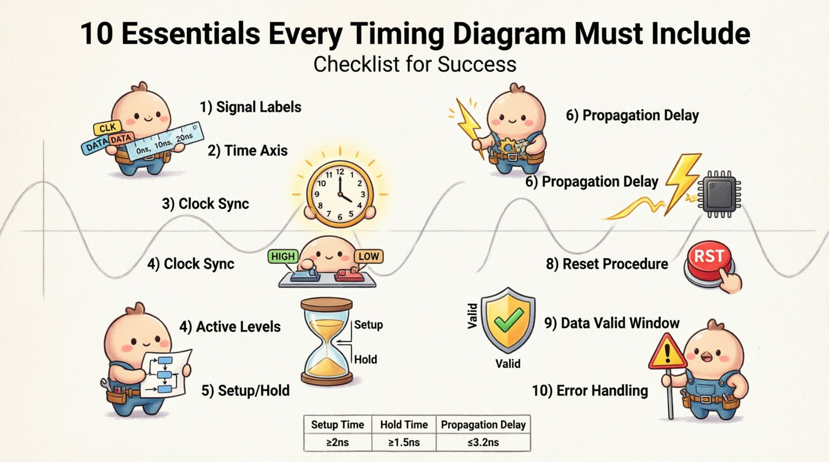
1. Clear and Unambiguous Signal Labels 🏷️
The foundation of any timing diagram is the ability to identify every signal uniquely. If a signal name is generic or missing, the diagram loses its utility. Every line in the diagram must correspond to a specific node in the circuit or protocol specification.
- Unique Naming: Avoid generic names like “Signal 1” or “Data.” Use the actual net names from the schematic, such as
UART_RX,I2C_SCL, orMEM_WR. - Consistency: Ensure the naming convention matches the documentation and the codebase. If the schematic uses
CS_N, do not label the diagram asChip_Select. - Directionality: Indicate the flow of data. While arrows are common in schematics, in timing diagrams, the label position relative to the waveform often implies direction. Explicitly state if a signal is input, output, or bidirectional in the legend.
- Bus Grouping: For wide buses, group signals logically. Use a bracket notation like
[7:0]to represent an 8-bit data bus without drawing eight separate lines, but ensure the individual bit transitions are clear in a zoomed-in view.
Failure to label signals correctly leads to misinterpretation. A verification engineer might simulate the wrong signal, and a software driver might be written for the wrong pin, causing integration failure.
2. Defined Time Axis and Scale ⏱️
A timeline without a scale is a sketch, not a diagram. The horizontal axis represents time, and without defined units, the relationships between signals are meaningless. The time axis must be clearly marked to allow for quantitative analysis of delays and cycles.
- Time Units: Always specify the unit of measurement. Common units include nanoseconds (ns), microseconds (μs), or clock cycles.
- Scale Markers: Include tick marks at regular intervals. For complex protocols, a grid background helps the eye track alignment vertically.
- Zoom Levels: A single diagram rarely shows the entire transaction. Use multiple views. A high-level view shows the overall transaction flow, while a zoomed-in view details the critical setup and hold windows.
- Start Time: Define the reference point. Is time zero the moment a clock edge occurs, or the moment a reset signal is asserted? Consistency in the zero-point is vital for comparing different test cases.
Without a defined scale, engineers cannot calculate propagation delays or verify that a system meets its frequency requirements. The time axis transforms the diagram from a qualitative illustration into a quantitative tool.
3. Explicit Clock Synchronization ⏰
Most digital systems rely on a clock signal to synchronize state changes. In asynchronous systems, clocks may be derived from different sources, but in synchronous designs, the clock edge is the anchor for all timing analysis. The clock must be clearly depicted and understood.
- Frequency and Period: State the clock frequency. If the period varies (jitter), indicate the range.
- Edge Triggering: Specify whether the logic is triggered on the rising edge (positive edge) or falling edge (negative edge) of the clock. This is often denoted by a triangle symbol at the base of the clock waveform.
- Duty Cycle: Indicate the ratio of high time to low time. A 50% duty cycle is standard, but many systems operate with asymmetric clocks.
- Clock Domains: If multiple clocks exist, clearly separate them. Show the relationship between different clock domains, including whether they are synchronous or asynchronous.
Missing clock information is a leading cause of timing violations. If a designer assumes a rising-edge trigger but the hardware is falling-edge, the data will be captured at the wrong moment, leading to metastability or incorrect state transitions.
4. Active High and Low Indicators 🔴🔵
Logic levels are not always intuitive. Some signals are active when high (1), while others are active when low (0). In many control lines, an active-low signal is denoted by a bar over the name (e.g., RESET_N), but visual representation in the diagram removes all doubt.
- Legend Requirement: Include a legend that defines what represents a logic high and a logic low. While high is typically the upper voltage level, voltage logic can vary (e.g., 3.3V vs 5V).
- Waveform Polarity: Use distinct visual cues. Active-low signals can be drawn with an inverted waveform or marked with a specific symbol (like a bubble) at the transition point.
- Idle States: Clearly define what the signal looks like when the device is not active. For example, a
Chip_Selectmight sit at a high logic level when inactive and drop low when selected. - Default Values: Specify the default state of tri-state buses. Are they floating, pulled up, or pulled down when not driven?
Confusion over active levels is a common source of hardware damage or logic failure. A signal meant to enable a peripheral might inadvertently disable it if the polarity is misinterpreted in the design phase.
5. Setup and Hold Time Requirements ⏲️⏳
These are the most critical timing parameters in synchronous design. Setup time is the duration before a clock edge that data must be stable. Hold time is the duration after the clock edge that data must remain stable. These windows define the reliability of data capture.
- Visualizing the Window: The diagram should explicitly highlight the setup and hold windows around the active clock edge. Shaded regions or dashed lines work well for this.
- Data Stability: Show that the data line does not change during these critical windows. Any transition during the setup or hold window risks a timing violation.
- Margin: Include a margin of safety. The diagram should show that the actual data transition occurs well outside the forbidden window, not just touching the edge.
- Derivation: If the timing is derived from a datasheet, reference the specific component or section. Different components have different tolerance requirements.
Ignoring setup and hold times is the primary cause of intermittent bugs in digital systems. These bugs may not appear during testing but can manifest under different temperature or voltage conditions, making them notoriously difficult to reproduce.
6. Propagation Delays ⚡
Signals do not travel instantaneously. There is always a delay between a change in an input and the corresponding change in an output. This delay is caused by gate propagation, trace length, and load capacitance. A complete timing diagram accounts for these latencies.
- Input to Output Delay: Measure and display the time between an input edge and the resulting output edge. This is critical for combinational logic paths.
- Trace Delay: In high-speed interfaces, the physical length of the wire contributes to delay. Include this in the analysis if the board layout affects timing.
- Skew: If multiple signals arrive at the same destination, show the skew (difference in arrival time). Excessive skew can violate setup or hold times even if individual paths are compliant.
- Path Delays: For complex paths, break down the delay into stages. This helps in debugging where the bottleneck occurs.
Without accounting for propagation delays, a design might appear to work in simulation but fail in hardware. Real-world physics dictates that signals take time to move, and the diagram must reflect this reality.
7. State Transitions and Sequencing 🔄
Many protocols and controllers operate in a sequence of states (e.g., Idle → Request → Acknowledge → Complete). The timing diagram must show the sequence of events clearly, linking the state of the control logic to the timing of the signals.
- State Labels: Label the timeline with state names above the waveforms. This helps correlate the signal activity to the logical state machine.
- Transitions: Clearly mark the boundaries between states. Is a state change immediate, or does it require a clock cycle?
- Wait States: If the system requires waiting (e.g., for memory to become ready), show the wait state explicitly as a period where no data changes occur.
- Dependencies: Show how one state enables the next. For example, a signal must go high before the next clock cycle begins.
State sequencing ensures that the protocol is followed correctly. A missing wait state or an incorrect state transition can cause the receiving device to read garbage data or lock up entirely.
8. Reset and Initialization Procedures 🛑
Before any communication or logic operation begins, the system must be in a known state. Reset sequences are often overlooked in timing diagrams, yet they are fundamental to system reliability. The diagram should cover the power-up or reset scenario.
- Reset Assertion: Show how long the reset signal is held active. Is it a pulse or a level? How long must it be held to ensure internal registers clear?
- Release Sequence: Show what happens when the reset is released. Do other signals need to be stable before the reset comes out?
- Startup Delay: Include any delay required for power rails to stabilize before the clock starts toggling.
- Initialization Values: If specific data is loaded into registers during reset, show this on the data lines immediately following the reset release.
A system that boots up unpredictably is a system that fails. By documenting the reset sequence, engineers ensure that every component starts from a defined baseline, reducing the risk of race conditions during power-up.
9. Data Valid Windows ✅
It is not enough to show a signal changing; the diagram must indicate when the data is actually valid and readable by the receiving logic. This concept is closely tied to the setup and hold times but focuses on the data validity itself.
- Valid Flag: If a protocol has a specific valid signal (like
VALIDin AXI orREADYin Avalon), show it explicitly. Data is only meaningful when the valid flag is high. - Stable Period: Highlight the period where the data lines remain constant. Transitions should not occur during this period.
- Eye Diagram Concept: While not an eye diagram, the timing diagram should conceptually show the “eye” where the data is safe to sample. The center of this window is the optimal sampling point.
- Handshake: In handshake protocols, show the relationship between the request, grant, and data valid signals. The data must be valid during the grant window.
Defining the valid window prevents race conditions. If the receiver samples data outside this window, it captures a transition rather than a stable value, leading to errors that are difficult to debug.
10. Error Conditions and Exceptions ❌
A perfect world does not exist. Timing diagrams should also document what happens when things go wrong. This includes error conditions, timeouts, and exception handling. This is often the most neglected part of the documentation.
- Timeouts: Define how long a system waits for a response before giving up. Show the timeout signal assertion.
- Error Signals: Show what happens when a parity error, CRC failure, or protocol violation occurs. Does the system halt? Does it retry?
- Retry Mechanisms: If a transaction fails, show the retry sequence. How much time is consumed before the next attempt?
- Deadlocks: Indicate scenarios where signals might hang. For example, if a device does not respond, the bus master should eventually release the bus.
Documenting error conditions prepares the system for real-world usage. It ensures that the error handling logic is designed to match the timing expectations, preventing the system from hanging indefinitely.
Timing Parameters Reference Table 📊
The following table summarizes the critical parameters discussed above to assist in quick verification during the design review process.
| Parameter | Description | Typical Unit | Impact of Error |
|---|---|---|---|
| Setup Time | Time data must be stable before clock edge | Nanoseconds (ns) | Metastability, Data Corruption |
| Hold Time | Time data must be stable after clock edge | Nanoseconds (ns) | Metastability, Data Corruption |
| Propagation Delay | Time for signal to travel through logic/trace | Nanoseconds (ns) | Timing Violation, Skew |
| Clock Period | Time between two consecutive clock edges | Nanoseconds (ns) | Frequency Mismatch, Overshoot |
| Reset Pulse Width | Duration of active reset signal | Nanoseconds (ns) | Uninitialized State, Boot Failure |
| Skew | Difference in arrival time of clock/data | Nanoseconds (ns) | Capture Error, Setup Violation |
Best Practices for Diagram Construction 🛠️
Beyond the ten essential elements, the overall quality of the timing diagram affects its usability. Follow these best practices to ensure the document serves as a reliable reference.
1. Consistent Alignment
Ensure all signals are aligned vertically where possible. Misaligned waveforms create visual noise and make it difficult to see relationships between signals. Use a grid to maintain alignment.
2. Logical Grouping
Group related signals together. Put all control signals (clock, reset, enable) at the top. Put data signals below. Put status signals at the bottom. This hierarchy helps the reader understand the flow of control versus the flow of data.
3. Annotation Clarity
Use text annotations sparingly but effectively. Do not clutter the diagram with excessive text. Instead, use callout lines to point to specific features like “Setup Window” or “Invalid Zone”.
4. Version Control
Timing diagrams evolve as the design evolves. Include a version number, date, and revision history in the footer of the document. This prevents teams from working off outdated specifications.
5. Cross-Referencing
Link the timing diagram to the relevant sections of the datasheet or protocol specification. If a timing requirement comes from a specific page in a component manual, cite it directly. This adds authority to the requirements.
Common Pitfalls to Avoid ⚠️
Even experienced engineers can make mistakes when creating timing diagrams. Being aware of common pitfalls helps maintain high standards.
- Ambiguous Transitions: Avoid drawing lines that slope diagonally between high and low states. Use vertical lines to indicate instantaneous transitions for digital logic, or clearly indicate rise/fall times if they are analog characteristics.
- Ignoring Jitter: Real clocks have jitter. If the system is high-speed, ignore the jitter at your peril. Indicate jitter bounds on the clock signal.
- Over-Simplification: Do not remove details just to make the diagram look cleaner. If a specific delay matters, draw it. If a wait state matters, include it.
- Lack of Context: A diagram without a title or description is useless. Always include a header that explains what transaction or scenario is being depicted.
Final Thoughts 🧭
Creating a timing diagram is an act of translation. It translates abstract electrical behavior into a visual language that humans can understand and engineers can verify. By incorporating the ten essentials outlined in this guide, you ensure that the translation is accurate, complete, and useful.
These elements form the bedrock of signal integrity and system reliability. They are not optional decorations; they are requirements for functional hardware. Whether you are designing a simple microcontroller interface or a complex high-speed memory bus, the principles remain the same. Precision, clarity, and completeness are the keys to success.
As you review your next design, use this checklist as a benchmark. Ensure every signal has a name, every time has a unit, and every state is defined. This discipline will save time, reduce errors, and result in systems that perform as intended. The effort invested in a high-quality timing diagram pays dividends throughout the entire product lifecycle.