Firmware development exists at the intersection of abstract logic and physical reality. While code executes in a logical sequence, hardware responds to voltage levels, clock cycles, and propagation delays. Without a clear visual representation of these interactions, even the most robust code can fail to communicate effectively with peripherals, sensors, or external systems. This is where the timing diagram becomes an essential artifact. It serves as the contract between the software logic and the physical electrical signals, ensuring that data is sampled correctly and commands are issued within the required windows.
A well-constructed timing diagram eliminates ambiguity. It defines exactly when a signal must rise, when data must be stable, and how long a processor must wait before proceeding. For engineers working on embedded systems, microcontrollers, or real-time applications, understanding how to map out these timelines is critical. This guide provides a structured approach to creating timing diagrams that accurately reflect your firmware timeline, ensuring reliability and preventing subtle race conditions.
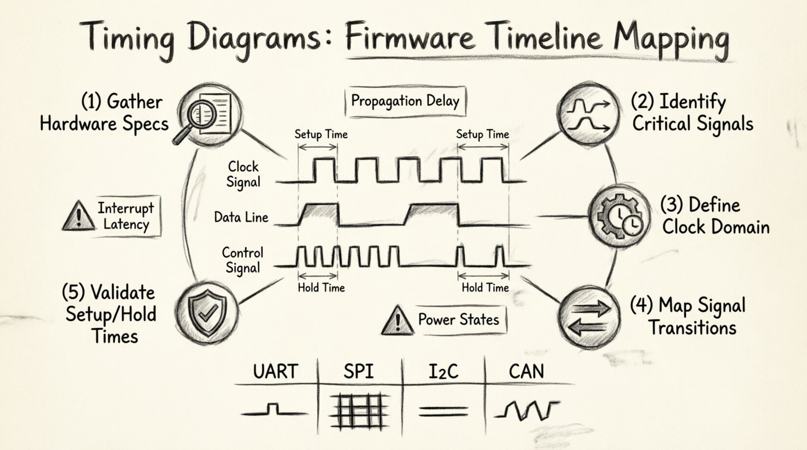
🧩 Understanding the Foundations of Timing Diagrams
Before diving into the mapping process, it is vital to understand what a timing diagram represents in the context of firmware. It is not merely a picture of waves; it is a temporal map of causality. Every transition on a signal line triggers a reaction elsewhere in the system. The diagram captures these relationships along a horizontal axis representing time.
- Time Axis: The horizontal line usually progresses from left to right, representing microseconds or nanoseconds.
- Signal Lines: Vertical tracks representing specific wires, buses, or logical states.
- Events: Specific points where a signal changes state, such as a clock edge or a data transition.
- Delays: The gap between a trigger and a response, often caused by propagation time or software latency.
When mapping firmware, you are essentially translating code execution flow into physical signal behavior. For instance, a function call in C code might take 50 clock cycles. In a timing diagram, this translates to a specific duration on the time axis during which a specific GPIO pin might hold a high state. This translation is the core challenge of the task.
⚙️ Why Precision Matters in Embedded Logic
Embedded systems often operate under strict constraints. Unlike general-purpose computing, where a slight delay might just slow down a user interface, embedded systems might control physical machinery, safety mechanisms, or communication protocols. A deviation of a few nanoseconds in a timing diagram can lead to data corruption, hardware damage, or system instability.
Consider a communication protocol like I2C. The master device must release the SDA line before the SCL clock line transitions. If the firmware takes too long to release the line, the slave device might interpret the signal incorrectly. The timing diagram defines the “window of opportunity” for this action. By mapping this out explicitly, you identify the constraints that the code must meet.
Key reasons for precision include:
- Signal Integrity: Ensuring voltage levels are met before sampling occurs.
- Bus Arbitration: Managing who controls the bus at any given moment.
- Interrupt Latency: Knowing how quickly the system responds to external events.
- Power Management: Coordinating sleep modes with wake-up signals.
📋 Phase 1: Gathering Hardware Specifications
The first step in mapping a timeline is gathering the ground truth. You cannot map a timeline without knowing the physical limits of the hardware. This phase involves collecting data from datasheets, schematics, and hardware manuals.
- Review Datasheets: Look for electrical characteristics. What are the maximum and minimum voltage levels for logic high and logic low? What are the rise and fall times?
- Identify Clock Frequencies: Note the system clock speed and the peripheral clock speeds. This determines the granularity of your time axis.
- Check Timing Constraints: Most peripherals have specific timing requirements. Look for sections labeled “AC Timing Characteristics” or “Electrical Specifications”.
- Understand Pin Multiplexing: If a pin can serve multiple functions, know which electrical characteristics apply to the firmware timeline.
This information forms the boundaries within which your firmware must operate. If the hardware requires a 10-microsecond delay between two actions, your diagram must reflect that gap.
📡 Phase 2: Identifying Critical Signals
Not all signals are created equal. In a complex system, there may be dozens of GPIO lines. Focusing on every single wire will clutter the diagram and obscure the critical path. You must identify the signals that dictate the flow of the firmware.
- Clock Signals: The heartbeat of the system. These define the timing resolution.
- Data Lines: The actual information being transferred.
- Control Lines: Signals like Chip Select, Ready, or Interrupt lines that dictate when data transfer can happen.
- Status Signals: Flags indicating completion or error states.
When creating the diagram, group these signals logically. For example, if you are mapping a SPI transfer, group the MOSI, MISO, SCK, and CS lines together. Do not mix them with unrelated power management signals unless the power state directly impacts the data transfer.
⏰ Phase 3: Defining the Clock Domain
Timing diagrams are meaningless without a reference for time. In firmware, this is usually the processor clock or a specific peripheral clock. Defining the clock domain helps in calculating the duration of software operations.
For example, if your microcontroller runs at 100 MHz, one clock cycle is 10 nanoseconds. If a loop takes 100 iterations, that is 1 microsecond. You can mark this on the diagram. However, you must account for:
- Pipeline Stalls: Modern processors might delay execution based on instruction dependencies.
- Bus Contention: If the CPU is waiting for memory access, the effective time for a signal change increases.
- Interrupts: High-priority interrupts can preempt the main flow, altering the timeline.
It is often helpful to mark the clock ticks on the horizontal axis. This provides a visual grid that helps estimate durations more accurately. If you cannot measure exact cycles, use conservative estimates based on the instruction set architecture documentation.
🔄 Phase 4: Mapping Signal Transitions
This is the core of the mapping process. You are now translating the logical steps of your code into physical signal changes. This requires a line-by-line analysis of the critical firmware routines.
- Start with the Trigger: Identify what initiates the sequence. Is it a button press? A timer interrupt? A received packet?
- Map the Setup: Before data is sent, what pins need to be configured? This might involve setting direction registers or enabling clocks. Mark these states on the diagram.
- Map the Execution: As the code executes, record when specific pins change. For example, when a loop writes to a register, does the GPIO pin toggle immediately? Or is there a buffer?
- Map the Wait: If the code calls a delay function, draw a flat line indicating the signal remains constant for that duration.
- Map the Teardown: After the operation, what pins are reset? This is crucial for protocols that require a specific idle state.
During this phase, pay attention to the edges of the signals. A rising edge might trigger a receiver. A falling edge might indicate the end of a byte. The diagram must clearly distinguish between stable states and transition periods.
⏳ Phase 5: Validating Setup and Hold Times
One of the most common causes of hardware failure is violating setup and hold times. These are the minimum times data must be stable before and after a clock edge. Your timing diagram must explicitly highlight these windows.
Setup Time: The time data must be valid before the clock edge. If your firmware takes too long to prepare the data, the hardware will sample garbage.
Hold Time: The time data must remain valid after the clock edge. If the firmware changes the line too quickly, the receiver might see a transition during the sampling window.
To validate this, draw vertical lines on your diagram to mark the clock edges. Then, draw vertical lines to mark the data validity windows. Ensure there is no overlap that violates the constraints. If the firmware logic is too tight, you may need to insert explicit wait states or optimize the code path.
📡 Common Communication Protocols
Different protocols have different timing requirements. When mapping firmware for these, you should reference standard timing diagrams for the protocol itself.
| Protocol | Key Timing Feature | Firmware Consideration |
|---|---|---|
| UART | Baud Rate Alignment | Ensure sampling occurs at the center of the bit window. |
| SPI | Clock Polarity & Phase | Match the clock edge where data is sampled and shifted. |
| I2C | Slew Rate & Hold Time | Allow enough time for the open-drain pull-ups to rise. |
| CAN | Bit Timing Segments | Configure the time quanta to match the network speed. |
When creating your diagram, label the protocol segments clearly. For SPI, indicate whether the data is valid before or after the clock edge. For I2C, mark the Start and Stop conditions distinctly. These visual markers help debug issues where the protocol fails silently.
🔍 Debugging Timing Violations
Even with a perfect diagram, real-world conditions may introduce noise or variance. When debugging, use the timing diagram as a baseline. If the system fails, compare the actual signal capture against the planned diagram.
- Check for Glitches: Short pulses that might be interpreted as valid edges. These often indicate signal integrity issues or switching noise.
- Analyze Jitter: Variations in the clock period. If the clock is jittery, your setup time margins shrink.
- Review Interrupt Overhead: If an interrupt fires during a critical timing window, it might delay the firmware response. Check if the interrupt latency fits within the allowed window.
- Validate DMA Transfers: Direct Memory Access can bypass the CPU. Ensure the DMA controller is not accessing memory while the CPU needs it, causing bus contention delays.
Debugging is often about finding the gap between the ideal diagram and the physical reality. The diagram helps you ask the right questions: Did the signal change too early? Did the clock edge arrive late? Was there a bus collision?
📝 Documentation and Handoff
A timing diagram is useless if it is not documented and versioned. It serves as a reference for future maintenance and for other team members. Treat it as a formal specification.
- Version Control: Keep the diagram file in the same repository as the firmware. Update it whenever the code logic changes.
- Annotations: Add notes explaining why certain delays exist. Was it for hardware initialization? For signal stabilization? This context is valuable for future engineers.
- Standards: Follow industry standards for drawing diagrams. Use consistent line weights, font sizes, and labeling conventions.
- Accessibility: Ensure the diagram is readable without specialized software. Export to PDF or image formats for easy sharing.
Documentation also includes the assumptions made. If the diagram assumes a specific load on the bus, note that. If it assumes a specific temperature range, record it. These constraints are part of the timing analysis.
⚠️ Common Pitfalls to Avoid
While creating these diagrams, there are common mistakes that can lead to inaccurate timelines. Being aware of them helps maintain the integrity of your work.
- Ignoring Propagation Delay: Wires and traces have physical length. Signals take time to travel. Do not assume zero delay between connected components.
- Assuming Instantaneous Code Execution: Compilers optimize code. A function might run faster than expected, or slower if it triggers cache misses. Measure actual execution time where possible.
- Overlooking Asynchronous Events: External inputs might arrive at unpredictable times. Your diagram should show the worst-case scenario for these events.
- Mixing Time Scales: Do not mix milliseconds and nanoseconds on the same axis without clear scaling indicators. This can lead to misinterpretation of signal durations.
- Neglecting Power States: A device in sleep mode might not respond to signals immediately. Map the transition from sleep to active state clearly.
🛠️ Best Practices for Maintenance
Timing diagrams are living documents. As the firmware evolves, the diagram must evolve with it. Here are some best practices to keep the diagram accurate over the lifecycle of the project.
- Review on Code Changes: Whenever a critical routine is modified, review the diagram. Does the new code still meet the timing requirements?
- Automate where Possible: If you have access to timing analysis tools, use them to verify the diagram automatically. This reduces human error.
- Collaborate with Hardware Engineers: Hardware engineers often have a different view of the timing constraints. Cross-check your diagram with their expectations.
- Keep it Simple: Do not add unnecessary signals. If a signal does not affect the critical path, leave it out to keep the diagram readable.
- Use Consistent Notation: Define a legend for symbols. Use the same arrow styles for data flow and the same line styles for clock signals throughout the document.
📐 Conclusion on Timeline Mapping
Creating a timing diagram for firmware is a discipline that bridges the gap between logic and physics. It requires a deep understanding of both the code execution flow and the electrical characteristics of the hardware. By following a structured method—gathering specifications, identifying signals, defining clock domains, mapping transitions, and validating constraints—you can create a reliable map of your system’s behavior.
This map is more than a drawing; it is a tool for validation, debugging, and communication. It ensures that when you write code, you know exactly how it will manifest in the physical world. It prevents the subtle bugs that arise from race conditions and timing violations. In the world of embedded systems, precision is the difference between a product that works and one that fails.
Take the time to document your timing. It will save hours of debugging later. Treat the timeline as a critical part of your design documentation, just as important as the schematic or the code itself. With a clear timing diagram, you gain confidence in your firmware, knowing that every signal transition is accounted for and every window of opportunity is respected.
Remember that technology evolves, but the fundamental need for synchronization remains. Whether you are working with legacy systems or cutting-edge microcontrollers, the principles of timing analysis remain the same. Apply these steps, maintain your diagrams, and ensure your firmware timeline is as robust as your hardware design.