In the complex ecosystem of Internet of Things (IoT) systems, data does not simply flow; it travels along specific pathways with strict temporal constraints. When microcontrollers, sensors, and cloud interfaces interact, the success of the operation depends less on the logic of the code and more on the precise timing of electrical signals. A timing diagram serves as the blueprint for this temporal coordination, illustrating how signals change over time relative to one another. Without a clear understanding of these diagrams, even the most sophisticated firmware will fail to transmit data accurately.
This guide explores the critical role of timing diagrams in ensuring reliable communication between IoT components. We will dissect the structure of these diagrams, analyze common protocols, and examine the physical realities that dictate signal behavior. By focusing on temporal precision, engineers can build systems that withstand noise, latency, and hardware variability.
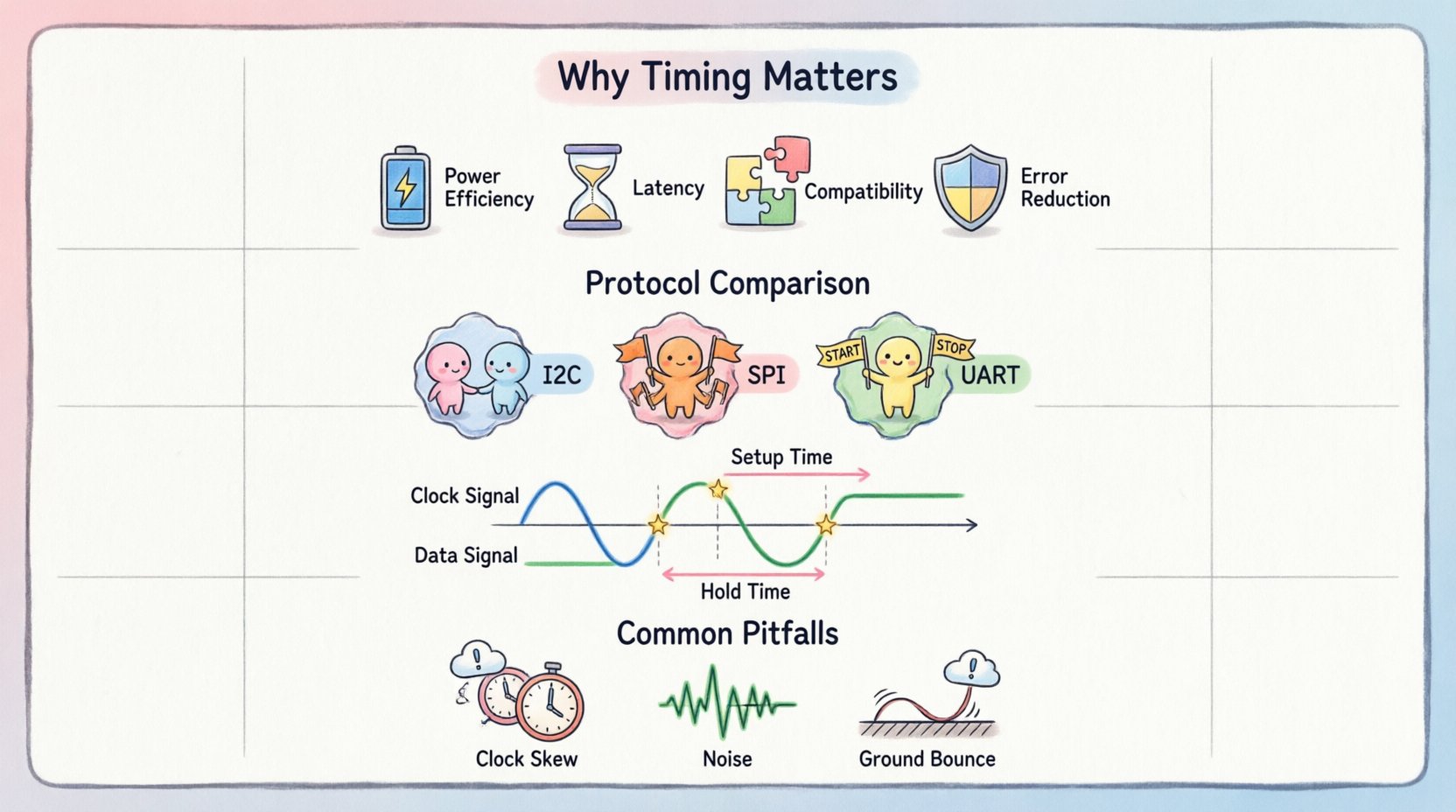
Why Temporal Precision Matters in IoT 🕒
IoT devices often operate in environments where resources are constrained. Power is limited, processing cycles are scarce, and bandwidth is expensive. In this context, timing is not merely a preference; it is a necessity. Every millisecond saved or lost has a direct impact on battery life, data throughput, and system stability.
- Power Efficiency: Sleep cycles and wake-up intervals rely on precise timers. If a device wakes up too early or too late, it may miss a transmission window or waste energy checking for data that is not there.
- Latency Management: In real-time applications like industrial automation or health monitoring, data must arrive within a specific window. Timing diagrams help visualize the end-to-end delay between sensing and actuation.
- Hardware Compatibility: Different chips operate at different clock speeds. A timing diagram ensures that a 3.3V logic output from one component is compatible with a 5V input on another, and that the transition speeds match.
- Error Reduction: Misaligned clocks lead to sampling errors. If a receiver samples a data line at the wrong moment, it reads a ‘1’ as a ‘0’, corrupting the packet.
Core Elements of a Timing Diagram 📐
Understanding the anatomy of a timing diagram is the first step toward mastering signal integrity. These diagrams are visual representations that plot voltage levels against time. They typically feature a horizontal axis representing time and a vertical axis representing voltage states.
The following components are fundamental to reading and creating these diagrams:
- Signals: These are the lines that represent physical wires or communication channels. Each signal has a name, such as SDA (Serial Data) or SCL (Serial Clock).
- Clock Cycles: Many protocols use a clock signal to synchronize data transfer. The rising and falling edges of this clock dictate when data should be sampled.
- Logic States: Digital signals exist in discrete states, typically Logic High (1) and Logic Low (0). In IoT, these levels correspond to specific voltage ranges (e.g., 0V to 0.8V for Low, 2V to 3.3V for High).
- Transitions: The change from High to Low or Low to High is critical. The speed of this transition affects electromagnetic interference (EMI) and signal quality.
- Setup and Hold Times: These are the windows before and after a clock edge where data must remain stable. Violating these times results in metastability or data corruption.
Visualizing Signal Relationships
When analyzing a diagram, the relationship between the clock and the data line is paramount. In some cases, data changes *before* the clock edge. In others, data changes *after*. Understanding this directionality prevents logical errors in design.
| Element | Description | Impact on System |
|---|---|---|
| Signal Line | A physical wire carrying voltage | Defines the path of data |
| Clock Edge | The moment a clock signal transitions | Triggers data sampling |
| Propagation Delay | Time taken for signal to travel | Affects maximum frequency |
| Setup Time | Time data must be stable before clock | Ensures valid reading |
| Hold Time | Time data must remain stable after clock | Prevents metastability |
Analyzing Synchronous vs. Asynchronous Communication 🔄
IoT systems utilize two primary methods for coordinating data exchange: synchronous and asynchronous. Timing diagrams differ significantly between these two modes, requiring distinct approaches to analysis and debugging.
Synchronous Communication
In synchronous communication, a shared clock signal controls the data flow. Both the transmitter and receiver agree on the timing based on this clock. This method allows for higher data rates but requires more wiring.
- Characteristics: Strict timing, high bandwidth, multi-wire requirement.
- Common Protocols: SPI (Serial Peripheral Interface), I2C (Inter-Integrated Circuit).
- Diagram Features: The clock line toggles continuously or on demand. Data bits are sampled on specific edges (rising or falling) of the clock.
- Advantages: High speed, no need for start/stop bits per byte, deterministic latency.
- Disadvantages: Clock skew can occur over long distances, requiring careful routing.
Asynchronous Communication
Asynchronous communication does not rely on a shared clock. Instead, both devices agree on a baud rate (bits per second) beforehand. Each data frame includes start and stop bits to mark boundaries.
- Characteristics: No clock line, lower bandwidth, simpler wiring.
- Common Protocols: UART (Universal Asynchronous Receiver-Transmitter), RS-232.
- Diagram Features: The line sits at a ‘Mark’ (High) state. A ‘Start’ bit pulls the line Low to initiate transmission. The receiver counts bits based on its internal clock.
- Advantages: Minimal wiring, robust over longer distances, flexible connection.
- Disadvantages: Lower speed, higher overhead due to start/stop bits, susceptible to baud rate mismatch.
Protocol-Specific Timing Requirements ⚙️
Different communication standards impose unique timing constraints. When designing an IoT node, selecting the right protocol depends heavily on these timing characteristics.
Inter-Integrated Circuit (I2C)
I2C is a two-wire protocol widely used for connecting low-speed peripherals. Its timing diagram is defined by specific voltage thresholds and clock stretching.
- Clock Frequency: Standard mode (100 kHz), Fast mode (400 kHz), High-speed mode (3.4 MHz).
- Bus Capacitance: The bus must not exceed a specific capacitance load, or rise times will slow down, violating timing specs.
- Hold Time: The SDA line must remain stable during the high period of the clock to ensure valid data.
- ACK/NACK: Timing diagrams must show the receiver pulling the SDA line low to acknowledge receipt.
Serial Peripheral Interface (SPI)
SPI is a full-duplex synchronous protocol. It uses separate lines for Master Out Slave In (MOSI), Master In Slave Out (MISO), and Clock (SCK).
- Phase and Polarity: Defined by CPOL (Clock Polarity) and CPHA (Clock Phase). These settings determine if data is sampled on the rising or falling edge.
- Chip Select: The CS line must be asserted (Low) before the clock starts and deasserted (High) after the transfer ends.
- Switching Time: Time taken for the master to change from output to input mode (or vice versa) on MISO/MOSI lines.
Universal Asynchronous Receiver-Transmitter (UART)
UART is the backbone of serial debugging and simple sensor connections. Its timing relies entirely on baud rate agreement.
- Start Bit: A transition from High to Low signals the beginning of a frame.
- Data Bits: Typically 8 bits, transmitted Least Significant Bit (LSB) first.
- Stop Bit: Returns the line to High, allowing the next frame to begin.
- Timing Margin: A 10% tolerance is standard. If the clocks drift beyond this, framing errors occur.
Comparison of Protocol Timing
| Protocol | Clock Requirement | Data Rate Limit | Typical Use Case |
|---|---|---|---|
| I2C | Yes (Shared) | Up to 3.4 MHz | Configuration registers, sensors |
| SPI | Yes (Dedicated) | Up to 50+ MHz | High-speed displays, memory |
| UART | No | Up to 1 Mbps | Debugging, GPS, Bluetooth |
| 1-Wire | No (Bit-banged) | 16.3 kbps | Temperature sensors, IDs |
Common Pitfalls and Error Analysis ⚠️
Even with a correct schematic, physical implementation often introduces timing errors. Debugging these issues requires a systematic approach using timing analysis.
- Clock Skew: In high-speed synchronous systems, the clock signal may arrive at different components at different times. If the skew exceeds the setup time, the data is sampled incorrectly.
- Rise/Fall Time Violations: If signals transition too slowly, they may linger in the undefined voltage region, causing the receiver to toggle unpredictably.
- Ground Bounce: Rapid switching of multiple outputs can cause the ground reference to shift momentarily. This changes the effective voltage levels, leading to false Low readings.
- Bus Contention: In open-drain configurations, if two devices drive the line simultaneously, timing glitches occur. The diagram should show only one device driving at a time.
- Intermittent Noise: Spikes on the data line can look like valid transitions. A timing diagram helps distinguish between noise (short duration) and data (sustained duration).
Optimizing for Power and Latency 🔋
IoT devices often run on batteries. Timing diagrams are not just for connectivity; they are tools for power management. By analyzing the active time of signals, engineers can optimize duty cycles.
Reducing Active Time
- Fast Transitions: Faster signal edges mean the line spends less time in the transition zone, reducing dynamic power consumption.
- Idle States: Ensure lines settle to a stable state (High or Low) when not in use. Floating lines consume more power due to leakage currents.
- Clock Gating: Disable the clock signal when data transfer is complete. The timing diagram should reflect periods where the clock is halted.
Minimizing Latency
- Buffer Sizes: Larger buffers reduce the frequency of interrupts but increase latency. Timing analysis helps find the balance.
- Polling vs. Interrupts: Polling requires continuous checking, adding overhead. Interrupts allow the system to sleep until data arrives. The timing diagram shows the latency between event and response.
Debugging Signal Integrity Issues 🛠️
When communication fails, the oscilloscope is the primary tool for viewing timing diagrams. Here is how to approach troubleshooting:
- Verify Voltage Levels: Ensure the High level meets the minimum input threshold and the Low level meets the maximum input threshold of the receiver.
- Check Edge Alignment: Align the clock edge with the data edge. If data changes in the middle of the clock high, the receiver will sample garbage.
- Look for Glitches: Short pulses between transitions indicate noise or ringing. These can cause false triggers.
- Measure Delay: Calculate the time difference between the master sending a command and the slave acknowledging. Excessive delay may indicate processing bottlenecks.
- Analyze Jitter: Jitter is the variation in the timing of signal edges. High jitter reduces the noise margin and can cause intermittent failures.
Design Guidelines for Robust Systems 🛡️
To prevent timing issues before they occur, adhere to these design principles during the schematic and layout phase.
- Impedance Matching: Match the trace impedance to the driver and receiver. Mismatches cause reflections that distort the timing diagram.
- Trace Length Matching: For synchronous buses, keep trace lengths equal to minimize skew. This is critical for high-speed SPI or parallel buses.
- Decoupling Capacitors: Place capacitors close to power pins to stabilize voltage during switching events. This prevents ground bounce from affecting timing.
- Shielding: Use ground planes to shield sensitive clock lines from noisy digital lines. Noise coupling can shift voltage thresholds.
- Termination Resistors: Use pull-up resistors for open-drain lines. Ensure the resistance value is low enough to drive the line fast but high enough to limit current.
Future Considerations in High-Speed IoT 🚀
As IoT devices become more capable, they require faster communication. The push towards 5G, Wi-Fi 6, and high-speed internal buses makes timing analysis more complex.
- Differential Signaling: Protocols like USB and Ethernet use differential pairs. Timing diagrams must show the relationship between the positive and negative lines to ensure common-mode rejection.
- Serializing Protocols: High-speed interfaces like PCIe or SATA serialize parallel data. Timing diagrams must account for the clock recovery embedded in the data stream.
- Wireless Synchronization: In wireless IoT (Bluetooth Low Energy, Zigbee), timing diagrams include air-interface slots. Jitter from the RF environment affects the precise timing of transmission windows.
Summary of Key Takeaways ✅
Timing diagrams are the foundation of reliable embedded communication. They provide a visual language for understanding how hardware components interact over time. By carefully analyzing setup times, hold times, and clock edges, engineers can design systems that operate stably under varying conditions.
Key points to remember include:
- Timing diagrams visualize voltage changes over time to ensure synchronization.
- Synchronous protocols use a clock, while asynchronous protocols rely on agreed-upon rates.
- Signal integrity issues like skew, jitter, and reflections can corrupt data.
- Power consumption is directly linked to signal transition speeds and idle states.
- Debugging requires oscilloscopes to capture real-world timing behavior.
Investing time in understanding these temporal relationships pays dividends in system reliability. Whether connecting a simple temperature sensor to a microcontroller or managing complex multi-node networks, the principles of timing remain constant. Precision in design leads to precision in operation.