Understanding how electronic components talk to each other is a fundamental skill in embedded systems engineering. One of the most critical tools for visualizing this communication is the timing diagram. These diagrams map out the relationship between signals over time, acting as a blueprint for how data moves across a circuit. For someone just starting out, these waveforms can look like a confusing mess of lines. However, once you understand the underlying logic, they become a powerful way to debug and design hardware. This guide breaks down timing diagrams into manageable concepts, using clear language and practical examples.
What Exactly Is a Timing Diagram? ⚙️
A timing diagram is a graphical representation of the relationship between two or more signals over time. In embedded systems, signals are electrical pulses that represent information. These diagrams show when a signal changes state (from low to high or vice versa) relative to other signals.
Think of it like a score for a musical piece. The vertical lines represent the instruments (signals), and the horizontal axis represents time. Just as a musician needs to know when to play a note to stay in sync with the band, an engineer needs to know exactly when to send or read data to ensure the system works correctly.
- Vertical Axis: Represents the signals (e.g., Clock, Data, Enable).
- Horizontal Axis: Represents time progression.
- Waveforms: The lines showing the voltage level of each signal.
Without these diagrams, debugging hardware communication would be like trying to fix a car engine by listening to the noise without seeing the parts. They provide a visual record of events that happen too fast for the human eye to see directly.
The Language of Signals: Voltage and Logic ⚡
Before reading the diagram, you must understand what the lines mean. In digital electronics, information is encoded using voltage levels.
Logic Levels
- Logic High (1): Usually represented by a higher voltage (e.g., 3.3V or 5V).
- Logic Low (0): Usually represented by a lower voltage (e.g., 0V or Ground).
It is important to note that the specific voltage thresholds can vary between different chips. Some chips might treat 2.5V as a high, while others might need 3.0V. The timing diagram abstracts this by showing binary states, but the physical reality involves voltage ranges.
Active High vs. Active Low
Some signals are active when they are high, while others are active when they are low. This is often indicated by a bubble (small circle) at the start of the signal name on the diagram.
- Active High: The function happens when the signal is at the top level.
- Active Low: The function happens when the signal is at the bottom level. This is common for reset signals or chip selects.
Key Components Explained 🧩
To read a timing diagram effectively, you need to identify specific features within the waveform.
Edges
Edges are the transitions where the signal moves from one level to another.
- Rising Edge: The signal goes from Low to High. Often used to trigger an action.
- Falling Edge: The signal goes from High to Low. Also used for triggering.
Period and Frequency
The clock signal is the heartbeat of the system. The time it takes to complete one full cycle (High + Low) is the period. The inverse of the period is the frequency, measured in Hertz (Hz).
Delay
No signal moves instantly. There is always a tiny delay between when a command is sent and when it is received. Timing diagrams explicitly show this gap, often labeled as t_pd (propagation delay).
Reading the Edges: Synchronization 🕒
In digital communication, the timing of when data is sampled is critical. There are two main approaches to synchronization:
Synchronous Communication
This method uses a dedicated clock signal to coordinate data transfer. The sender and receiver both follow the same clock rhythm.
- Example: SPI (Serial Peripheral Interface).
- Benefit: Precise timing and higher speeds.
- Drawback: Requires more wires (at least three: Data, Clock, Chip Select).
Asynchronous Communication
This method does not use a shared clock. Instead, both devices agree on a speed beforehand (baud rate) and start/stop bits mark the beginning and end of a byte.
- Example: UART (Universal Asynchronous Receiver-Transmitter).
- Benefit: Fewer wires needed (often just two).
- Drawback: Slightly more complex to handle errors if clocks drift.
Common Communication Protocols 📡
Timing diagrams are most often used to define and debug standard communication protocols. Here is a breakdown of three common ones.
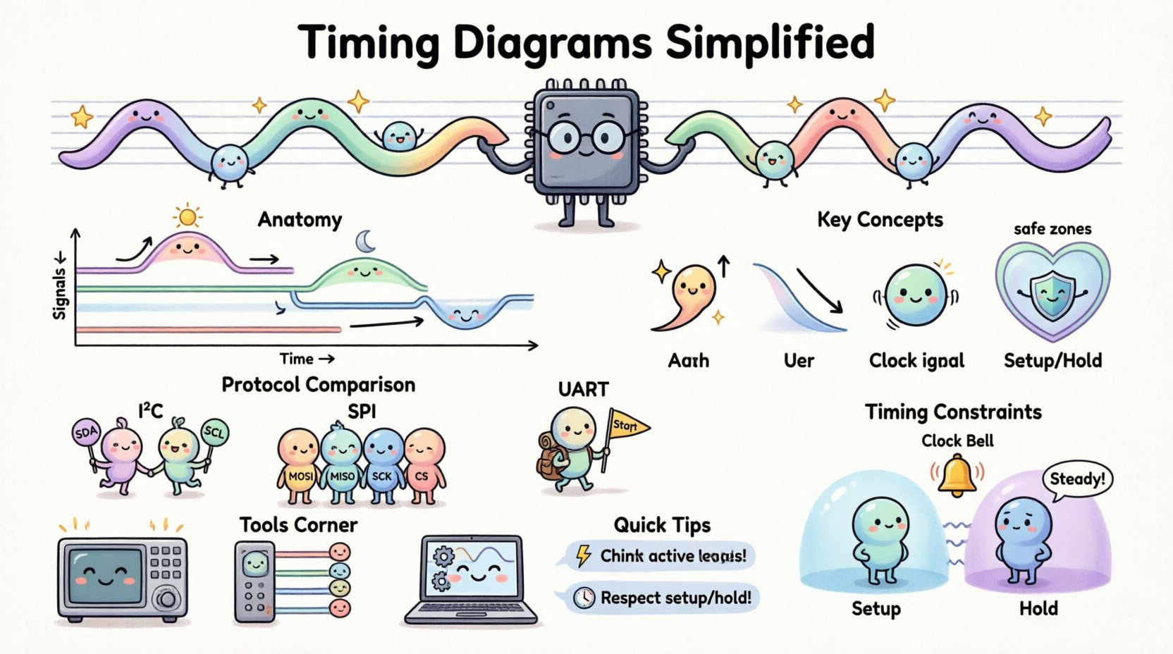
1. I2C (Inter-Integrated Circuit)
I2C is a popular protocol for connecting low-speed peripherals to a microcontroller. It uses two wires: SDA (Data) and SCL (Clock).
| Event | Signal Behavior |
|---|---|
| Start Condition | SDA goes High to Low while SCL is High. |
| Stop Condition | SDA goes Low to High while SCL is High. |
| Write | SDA is driven by the Master. |
| Read | SDA is driven by the Slave. |
| Acknowledge | Receiver pulls SDA Low during the clock pulse. |
Notice how the data line (SDA) must remain stable while the clock line (SCL) is High. If SDA changes while SCL is High, the system might interpret it as a Start or Stop condition.
2. SPI (Serial Peripheral Interface)
SPI is faster than I2C and uses four main signals: MOSI (Master Out Slave In), MISO (Master In Slave Out), SCK (Clock), and CS (Chip Select).
- Chip Select: Must be Low to activate the device.
- Clock Polarity (CPOL): Determines if the idle state is High or Low.
- Clock Phase (CPHA): Determines if data is sampled on the rising or falling edge.
When reading an SPI timing diagram, look for the Chip Select going low. Data transfer only happens while the Chip Select is active. The Clock signal dictates the speed of the data bits shifting out.
3. UART (Universal Asynchronous Receiver-Transmitter)
UART is the simplest serial protocol. It sends data one byte at a time without a clock.
- Idle State: The line stays High.
- Start Bit: A single Low pulse indicates the start of data.
- Data Bits: 8 bits typically, sent Least Significant Bit first.
- Stop Bit: Returns the line to High to signal the end.
Timing diagrams for UART focus heavily on the duration of the Start Bit. Since there is no clock, the receiver must rely on the precise timing of the start pulse to know when to sample the subsequent bits.
Timing Constraints: Setup and Hold Time ⏳
One of the most critical aspects of timing diagrams involves the relationship between data and the clock. Chips have physical limits on how fast they can process signals. These limits are defined by setup and hold times.
Setup Time
Setup time is the minimum amount of time the data signal must be stable before the clock edge arrives. If the data changes too close to the clock edge, the receiving chip might not register the value correctly.
Hold Time
Hold time is the minimum amount of time the data signal must remain stable after the clock edge has passed. This ensures the signal has settled enough to be latched into the memory cell.
Propagation Delay
This is the time it takes for a signal to travel from the input of a component to its output. In a timing diagram, you might see a gap between the clock edge and the data output. This gap is the propagation delay.
| Constraint | Definition | Failure Mode |
|---|---|---|
| Setup Time | Data stable before clock edge. | Metastability or incorrect capture. |
| Hold Time | Data stable after clock edge. | Glitching or race conditions. |
| Propagation Delay | Time for signal to travel. | Slower overall system speed. |
How to Analyze a Diagram Step-by-Step 📝
When you encounter a new timing diagram, follow this systematic approach to avoid confusion.
- Identify the Signals: Look at the labels on the left. Which are inputs, outputs, or control lines?
- Find the Clock: Locate the periodic signal. This sets the pace.
- Determine Active Levels: Check for bubbles or text indicating if High or Low is the active state.
- Trace the Sequence: Follow the timeline from left to right. Look for Start conditions, data transfers, and Stop conditions.
- Check Margins: Look for the setup and hold time requirements. Ensure the data lines are stable during the critical window.
- Look for Anomalies: Are there glitches? Are the pulses shorter than specified? These indicate potential hardware faults.
Common Mistakes for Beginners 🚫
Even experienced engineers can miss details. Here are common pitfalls to avoid.
- Ignoring Voltage Levels: Assuming 3.3V logic works with 5V devices without a level shifter can damage components.
- Misreading Edges: Confusing rising edges with falling edges can reverse the data flow logic.
- Overlooking Active Low: Assuming a signal is active High when it is actually Active Low can lead to devices never turning on.
- Neglecting Timing Margins: Designing for the exact edge of a constraint without room for error can cause systems to fail under temperature changes or voltage drops.
Tools for Visualization 🛠️
While you can draw these diagrams on paper, real-world debugging requires tools that capture actual electrical signals.
Oscilloscopes
An oscilloscope displays voltage over time. It is the most direct way to see a timing diagram in real life. You connect probes to the wires and watch the waveforms appear on the screen.
Logic Analyzers
A logic analyzer is designed specifically for digital signals. It captures multiple digital channels simultaneously and converts them into a clean timing diagram view. This is often easier to read than the analog wiggles of an oscilloscope.
Simulation Software
Before building hardware, engineers often simulate circuits. These tools generate timing diagrams automatically based on the code and circuit design. This allows you to catch errors before soldering any components.
Practice Exercises to Build Confidence 🧠
The best way to learn is by doing. Try these exercises to reinforce your understanding.
- Exercise 1: Find a datasheet for a common sensor (like an accelerometer). Locate the timing diagram for the interface and try to draw it from memory.
- Exercise 2: Use a logic analyzer to capture a simple SPI transaction. Compare the captured waveform to the datasheet diagram.
- Exercise 3: Calculate the maximum frequency for a system given a specific setup time and propagation delay.
- Exercise 4: Draw a timing diagram for an I2C Write operation to a specific register address.
Understanding Data Encoding 📊
Signals don’t just carry 1s and 0s; they carry meaning. How those bits are grouped matters.
MSB vs. LSB First
When sending a byte, do you send the most significant bit first or the least significant bit first? This is a common configuration setting. A timing diagram will show the sequence of bits clearly. If you expect MSB first but the diagram shows LSB first, your data will be misinterpreted.
Parity and Error Checking
Some protocols add extra bits to check for errors. A parity bit might be added to ensure the number of 1s is even or odd. Timing diagrams will show these extra bits following the main data payload.
Dealing with Noise and Glitches 🌪️
In the real world, signals are never perfect. Electromagnetic interference can cause voltage spikes or dips. These are called glitches.
A timing diagram helps identify these issues. If you see a spike on a data line that shouldn’t be there, it indicates noise. If a pulse is too narrow, the chip might not recognize it as a valid signal.
Filtering Strategies
- Hardware Filtering: Adding capacitors to smooth out voltage spikes.
- Software Debouncing: Ignoring signals that are too short in duration.
- Shielding: Using shielded cables to reduce external interference.
The Importance of Documentation 📄
Why do datasheets include these diagrams? They serve as the contract between the manufacturer and the user. If you follow the timing diagram exactly, the device will work as intended.
If you deviate from the diagram (e.g., by changing the clock speed), you risk violating the timing constraints. This can lead to unpredictable behavior. Always refer to the latest version of the timing diagram, as revisions can change electrical characteristics.
Final Thoughts on Signal Integrity 🏁
Mastering timing diagrams is a journey, not a destination. They are the bridge between abstract code and physical reality. As you design more complex systems, the diagrams will become more intricate, but the fundamental principles remain the same.
By paying attention to edges, levels, and constraints, you ensure that your embedded systems communicate reliably. Whether you are debugging a simple sensor or designing a high-speed interface, the timing diagram is your map. Treat it with respect, read it carefully, and let it guide your hardware decisions.
Remember, every line on that graph represents a physical voltage change. Understanding that connection is what separates a hobbyist from a professional engineer. Keep practicing, keep measuring, and let the signals guide you.