In the world of Internet of Things (IoT) development, the invisible dance between hardware and software determines success. At the heart of this synchronization lies the timing diagram. These visual representations are not just sketches; they are the blueprints for signal integrity and data reliability. For engineers working on embedded systems, understanding how to read and create timing diagrams is a fundamental skill. This guide explores the mechanics of timing constraints, signal relationships, and how to maintain stability in resource-constrained environments.
What is a Timing Diagram? 🔍
A timing diagram is a graphical representation of signals over time. It shows the relationship between different electrical signals in a system. In IoT contexts, these signals often represent data transmission between a microcontroller and a peripheral device like a sensor or a wireless module.
Unlike a flowchart which shows logical steps, a timing diagram focuses on when events happen. It visualizes:
- High and Low voltage states (Logic 1 and Logic 0)
- Clock pulses that drive the system
- Data transitions on input/output lines
- Setup and hold requirements for data capture
- Latency and propagation delays
By mapping these elements, engineers can predict how a circuit behaves under load. This is critical when dealing with low-power devices where every microsecond counts.
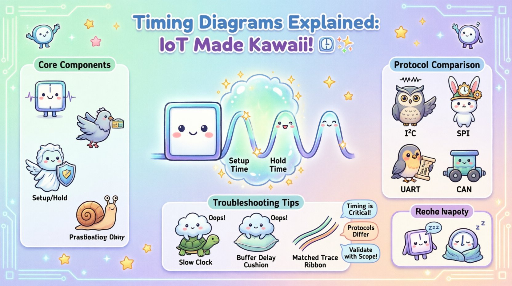
Core Components of Timing Analysis 🛠️
To interpret these diagrams effectively, one must understand the vocabulary of timing. Here are the essential elements you will encounter:
1. Clock Signals ⏱️
The clock is the heartbeat of synchronous systems. It dictates the pace at which data is sampled. In a timing diagram, the clock is often a square wave toggling between high and low.
- Frequency: How many cycles occur per second (Hz).
- Duty Cycle: The percentage of time the signal is high versus low.
- Edge: The transition point (rising or falling) where data is typically sampled.
2. Data Lines 📡
These lines carry the actual information. They change state based on the protocol rules. In a diagram, you will see them transitioning at specific times relative to the clock edge.
3. Setup and Hold Times ⏲️
These are the most critical constraints for data integrity.
- Setup Time: The minimum amount of time the data signal must be stable before the clock edge arrives.
- Hold Time: The minimum amount of time the data signal must remain stable after the clock edge arrives.
If these windows are violated, the receiving device may read incorrect data, leading to system errors or crashes.
4. Propagation Delay ⏳
Signals do not travel instantly. There is a delay between the input of a signal and the output response. In timing diagrams, this appears as a gap between the trigger event and the resulting action. In high-speed IoT links, this delay accumulates and must be accounted for.
Timing Constraints in IoT Environments 🌐
IoT devices operate differently than desktop computers. They often run on batteries, have limited processing power, and exist in electrically noisy environments. These factors introduce unique timing challenges.
Power vs. Speed Trade-offs 🔋
Reducing power consumption often means lowering clock speeds. When you slow down a clock to save energy, you must ensure that the timing windows for communication protocols remain valid. A diagram helps visualize if a lower frequency will cause data loss.
Noise and Interference 📉
Wireless modules and switching power supplies create electrical noise. This noise can cause signal jitter, which is the deviation of the signal edges from their ideal positions. Timing diagrams allow engineers to measure jitter and determine if it falls within acceptable limits.
Asynchronous Communication 🔄
Not all IoT communication relies on a shared clock. Protocols like UART are asynchronous. In these cases, timing diagrams show the start bit, data bits, parity, and stop bit. The receiver must estimate the timing based on a baud rate agreement. Deviations in oscillator accuracy can lead to framing errors.
Common Communication Protocols & Timing 📋
Different protocols have different timing requirements. Below is a comparison of how data moves in popular IoT interfaces.
| Protocol | Synchronization | Key Timing Characteristic | Typical Use Case |
|---|---|---|---|
| I2C | Synchronous | Open-drain lines with pull-up resistors; requires careful rise/fall time control. | Connecting sensors to microcontrollers on a PCB. |
| SPI | Synchronous | Faster than I2C; requires separate clock line; strict setup/hold times. | High-speed data from flash memory or displays. |
| UART | Asynchronous | Relies on fixed baud rate; no clock line; vulnerable to clock drift. | Serial debugging and simple command links. |
| CAN Bus | Synchronous | Differential signaling; arbitration based on timing of bits. | Automotive and industrial control networks. |
When designing a system, selecting the right protocol depends on the timing budget available. SPI offers speed but consumes more pins and power. I2C is efficient but slower due to rise time limitations.
How to Read a Timing Diagram 📖
Reading these diagrams requires a systematic approach. Follow these steps to analyze a signal trace effectively.
- Identify the Reference Signal: Usually, the clock is the top line. Align all other signals relative to its edges.
- Check Voltage Levels: Ensure the high and low levels match the logic standards (e.g., 3.3V vs 5V logic).
- Measure Time Intervals: Look at the distance between transitions. Are they within the spec sheet limits?
- Look for Anomalies: Do any lines glitch? Is there a spike that shouldn’t be there? These indicate noise or grounding issues.
- Verify Control Signals: Check enable lines, chip selects, and reset signals to ensure they activate at the correct moments.
Troubleshooting Timing Violations 🚨
Even with careful planning, timing violations can occur. When a device fails to communicate, a timing diagram analysis is the first line of defense. Here are common issues and how to spot them.
1. Setup Violation
This happens when data arrives too late before the clock edge. The receiver samples the data before it has settled. Visually, you will see the data transition overlapping the clock edge.
- Solution: Slow down the clock frequency or add delay to the data path.
2. Hold Violation
This occurs when the data changes too quickly after the clock edge. The receiver is still trying to latch the old value when the new value arrives.
- Solution: Increase the hold time margin by adding buffer delays or ensuring the driver is strong enough to maintain the signal.
3. Skew
Skew is the difference in arrival time between two signals. If the clock and data arrive at different times due to trace length differences, skew occurs.
- Solution: Route traces to match lengths. Use matched impedance routing techniques.
4. Metastability
This is a state where a flip-flop cannot decide between a 0 or 1. It usually happens when asynchronous signals cross clock domains. The output hovers in an undefined voltage range.
- Solution: Use synchronization chains (two or more flip-flops) to allow the signal to settle before being used.
Best Practices for Design Documentation 📝
Clear documentation prevents errors in production. When creating timing diagrams for your project, adhere to these standards.
- Use Standard Symbols: Follow industry conventions for clock edges and data states.
- Annotate Time Scales: Clearly label the horizontal axis (e.g., ns, µs, ms).
- Include Worst-Case Scenarios: Draw diagrams for maximum load and minimum voltage conditions.
- Version Control: Keep track of changes. A timing requirement update in hardware needs a corresponding update in the diagram.
- Collaborate with Firmware: Ensure the software team knows the exact timing constraints to avoid writing code that violates hardware limits.
The Role of Oscilloscopes in Validation 🔬
While diagrams are theoretical, validation requires hardware. An oscilloscope is the primary tool for verifying timing diagrams in the real world. It captures the actual waveforms.
When comparing the captured waveform to the design diagram, look for:
- Rise and Fall Times: Are they too slow? This can cause logic errors.
- Overshoot and Undershoot: Voltage spikes that exceed the power rails can damage components.
- Ground Bounce: Noise on the ground line that shifts the reference voltage.
- Jitter: Random variations in the clock signal timing.
Optimizing for Low Power IoT ⚡
Power management is a major driver in IoT design. Timing diagrams help optimize this by showing idle periods.
1. Duty Cycling
By analyzing the timing, you can schedule the device to sleep between transmissions. The diagram shows exactly how long the radio needs to be active, allowing for longer sleep cycles.
2. Clock Gating
Disabling the clock to unused peripherals saves energy. The timing diagram shows which blocks are active and when they can be safely gated off without losing data integrity.
3. Interrupt Latency
IoT devices often rely on interrupts to wake up. The timing diagram must account for the latency between the interrupt trigger and the processor waking up. If the timing is too loose, the sensor data might be missed.
Advanced Considerations: Multi-Domain Systems 🧩
Complex IoT systems often mix analog and digital domains. Analog sensors produce continuous signals that are converted to digital values. Timing diagrams must account for the conversion time of the Analog-to-Digital Converter (ADC).
Key Considerations:
- Sample-and-Hold: The time required to capture the analog voltage.
- Conversion Time: How long the ADC takes to output the digital number.
- Buffering: Whether the digital value is stored in a register before being read.
Ignoring these steps can lead to reading stale or incorrect data. The timing diagram acts as the bridge between the physical world and the digital logic.
Ensuring Signal Integrity in High-Speed Links 🚀
As IoT devices move toward higher data rates, signal integrity becomes paramount. High-frequency signals behave differently due to transmission line effects.
- Impedance Matching: Prevents reflections that distort the waveform.
- Trace Length: Longer traces introduce more capacitance and delay.
- Via Stubs: Unused via holes can act as antennas, reflecting energy back into the line.
A timing diagram for high-speed links often includes eye diagrams, which show the opening of the signal eye. A closed eye indicates significant timing jitter or noise.
Summary of Key Takeaways ✅
Understanding timing diagrams is essential for building reliable IoT systems. It provides a visual language for discussing signal behavior across hardware and software teams.
Remember these core points:
- Timing is Critical: Data must be stable during specific windows relative to the clock.
- Protocols Differ: Each communication standard has unique timing rules.
- Environment Matters: Noise, power, and temperature affect signal behavior.
- Validation is Key: Simulate the diagram, then measure it with real hardware.
- Document Clearly: Use diagrams to communicate constraints to the entire team.
By mastering the ability to read and create these diagrams, you ensure that your devices function correctly in the field. This reduces debugging time and increases the overall reliability of your product. In the complex ecosystem of connected devices, precision is the difference between a working product and a failed deployment.