Embedded systems rely on precise coordination between hardware and software. When firmware interacts with peripherals, sensors, or communication buses, timing becomes the invisible framework that dictates success or failure. For new firmware engineers, understanding how signals behave over time is critical. This guide breaks down the mechanics of reading timing diagrams, ensuring you can analyze signal integrity and protocol compliance with confidence. 🛠️
Why Timing Diagrams Matter in Firmware Development ⚙️
Hardware engineers design circuits to operate within specific electrical constraints. Firmware engineers write code to control these circuits. The intersection point is the timing diagram. Without this visual language, debugging hardware interactions becomes guesswork. A timing diagram provides a snapshot of voltage levels across multiple signals over a defined time interval. It reveals:
- Signal Transitions: When a wire goes from low to high or vice versa.
- Delays: How long it takes for data to propagate.
- Dependencies: Which signal must occur before another.
- Violations: Moments where signals break protocol rules.
By mastering this visual tool, you reduce the risk of race conditions, data corruption, and system instability. It bridges the gap between abstract code and physical reality. 🌉
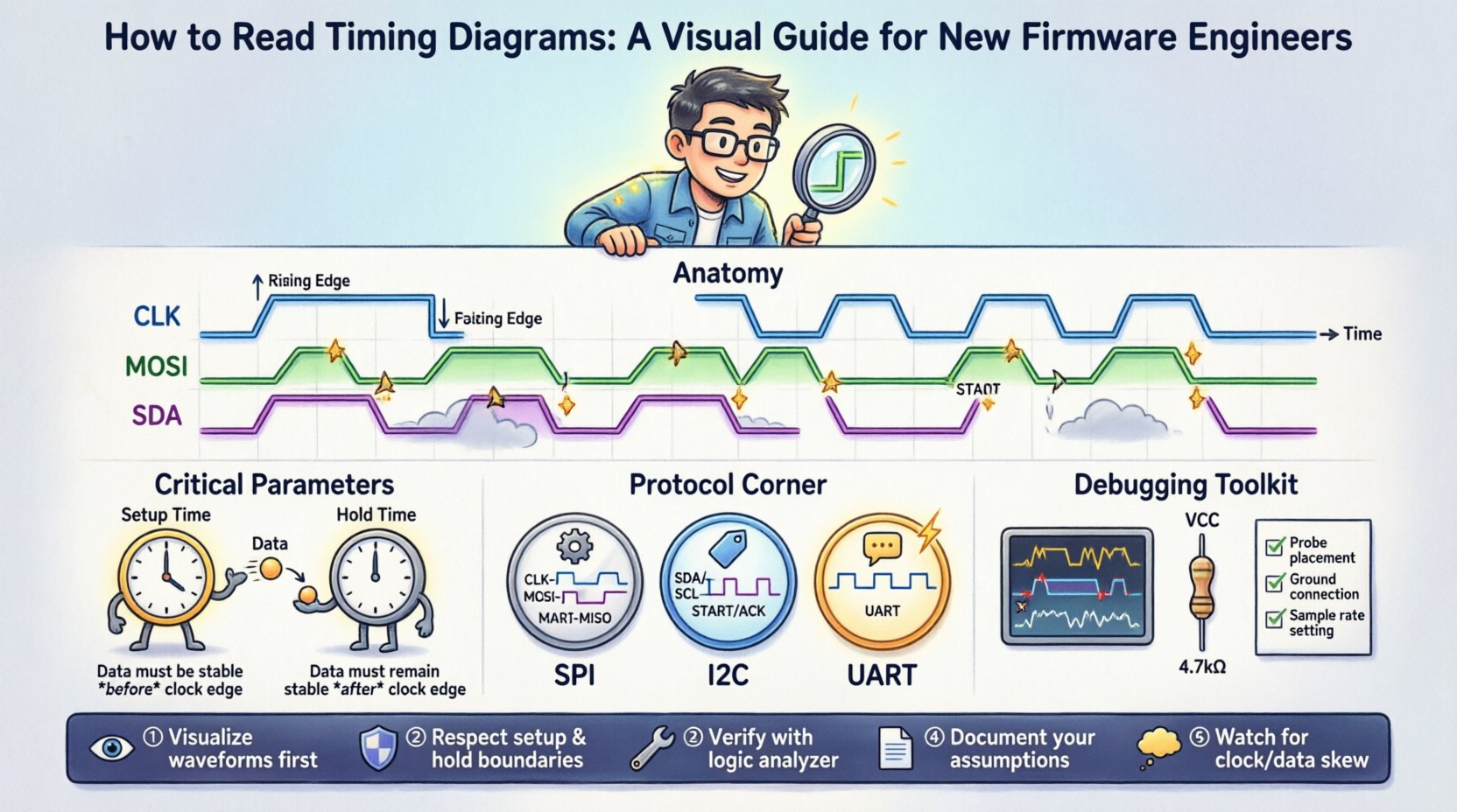
Anatomy of a Timing Diagram 🔍
Every timing diagram shares a common structure. Understanding these components is the first step toward interpretation. While styles vary, the core elements remain consistent across datasheets and logic analyzer exports.
1. The Time Axis ⏳
The horizontal axis represents time. It typically flows from left to right. Key characteristics include:
- Direction: Time always moves forward.
- Scale: May be linear (microseconds) or zoomed (nanoseconds).
- Markers: Vertical lines often denote specific events or clock edges.
2. Signal Lines 📉
Vertical lines represent individual wires or data lines. Each line is labeled to identify its function (e.g., CLK, SDI, CS). The state of the line is shown as:
- High (Logic 1): Usually represented by the top portion of the waveform.
- Low (Logic 0): Represented by the bottom portion of the waveform.
- High Impedance (Hi-Z): Sometimes shown as a dashed line or a specific color, indicating the pin is disconnected electrically.
3. Transitions and Edges 🔄
Signals do not switch states instantly. The transition from low to high is a rising edge. The transition from high to low is a falling edge. These edges often trigger actions in the receiving device. Timing diagrams show the slope of these transitions, indicating rise time and fall time.
Critical Timing Parameters 📏
Some parameters appear frequently in datasheets and must be understood to ensure reliable operation. These define the window of opportunity for data to be valid.
Setup Time ⏰
Setup time is the minimum amount of time a data signal must be stable before a clock edge. If data changes too close to the clock edge, the receiving device may not register the value correctly. Think of it as preparing your hands before catching a ball.
- Rule: Data must be stable for $T_{setup}$ before the clock edge.
- Violation: If violated, the device might read a random value.
Hold Time ⏱️
Hold time is the minimum amount of time a data signal must remain stable after a clock edge. The device needs to latch the value securely. If the data changes immediately after the clock edge, the previous value might be lost.
- Rule: Data must remain stable for $T_{hold}$ after the clock edge.
- Violation: Can lead to metastability or incorrect latching.
Propagation Delay ⚡
This is the time it takes for a signal to travel from the input of a component to its output. In high-speed firmware, this delay accumulates. If a signal travels too far, it may arrive too late for the next stage to process it.
Clock Period and Frequency 🎵
The clock period is the time between two consecutive rising edges. Frequency is the inverse of the period. Firmware loops often synchronize with the clock. Understanding the period ensures your code executes at the intended speed.
Reading Common Protocols 📡
Communication protocols have specific timing requirements. Below are examples of how to interpret diagrams for common interfaces.
Serial Peripheral Interface (SPI) 🔄
SPI uses a master-slave architecture. It typically includes a clock line (SCK), a master-out-slave-in line (MOSI), and a master-in-slave-out line (MISO). Chip select (CS) controls which device is active.
- Chip Select: Goes low to start communication, high to end.
- Clock Edges: Data is usually sampled on the rising or falling edge, depending on the mode.
- Timing: Data is valid before the clock edge (setup) and remains valid after (hold).
Inter-Integrated Circuit (I2C) 🏷️
I2C uses two wires: Serial Clock (SCL) and Serial Data (SDA). It is bidirectional and open-drain. Timing is crucial for synchronization.
- Start Condition: SDA goes low while SCL is high.
- Stop Condition: SDA goes high while SCL is high.
- Data Validity: Data must be stable when SCL is high. Changes only occur when SCL is low.
Universal Asynchronous Receiver/Transmitter (UART) 📟
UART is asynchronous, meaning it does not use a shared clock line. Instead, it relies on a predefined baud rate. Timing diagrams here focus on the bit duration.
- Start Bit: A low signal indicates the beginning of a frame.
- Data Bits: Sent least significant bit first.
- Stop Bit: Returns the line to high, signaling the end of the frame.
Comparing Protocol Timing Requirements 📊
Different protocols have different strengths regarding speed and complexity. Use this table to compare general timing characteristics.
| Protocol | Clock Required? | Direction | Typical Speed Range | Key Timing Constraint |
|---|---|---|---|---|
| SPI | Yes (Master) | Full-Duplex | Up to 50 MHz | Clock Duty Cycle & Setup/Hold |
| I2C | Yes (Bidirectional) | Half-Duplex | 100 kHz to 3.4 MHz | Bus Capacitance & Low Time |
| UART | No | Half-Duplex | 9600 to 115200 baud | Baud Rate Tolerance |
| Parallel Bus | Yes | Full-Duplex | Variable | Skew & Propagation Delay |
Analyzing Clock Domains and Skew ⏱️🚫
When multiple clocks exist in a system, timing analysis becomes complex. This is known as crossing clock domains.
Clock Skew 📐
Clock skew is the difference in arrival times of the clock signal at different parts of the circuit. If the clock reaches one flip-flop earlier than another, the setup time calculation changes. Firmware engineers must account for this when configuring peripherals.
Phase Shift 🔄
Two clocks may run at the same frequency but start at different points in their cycle. If data is transferred between them without proper synchronization, data loss occurs.
Metastability ⚠️
If a signal violates setup or hold time, the receiving flip-flop may enter a metastable state. The output becomes unpredictable, oscillating between high and low before settling. This can cause system crashes. Mitigation involves using synchronizer circuits (two flip-flops in series) to allow time for the signal to settle.
Debugging Timing Violations 🛠️🔍
When firmware fails to communicate with hardware, a timing violation is a common suspect. Follow this process to diagnose the issue.
- Verify Wiring: Check for loose connections or short circuits that distort signal edges.
- Check Pull Resistors: Open-drain protocols like I2C require pull-up resistors. Missing resistors cause slow rise times, violating timing specs.
- Analyze Signal Slope: Use a logic analyzer to view the actual transition time. Slow edges may look like logic errors.
- Review Code Timing: Ensure your firmware loop does not block the clock signal for too long.
- Adjust Interrupts: High-priority interrupts can delay peripheral handling, causing missed deadlines.
Best Practices for Firmware Documentation 📝
Clear documentation helps future engineers understand the timing constraints you implemented.
- Annotate Delays: Document any explicit delays in code and explain why they are necessary.
- Link to Datasheets: Always reference the specific timing section of the hardware datasheet.
- Include Diagrams: If a protocol is complex, include a simplified timing diagram in the documentation.
- State Assumptions: Note assumptions about clock stability or temperature ranges.
Understanding Logic Analyzer Readouts 🔬
Logic analyzers are the primary tool for verifying timing diagrams. They capture digital signals and display them as waveforms.
Triggering 🎯
Triggering allows you to capture specific events. For example, you can set the analyzer to stop recording when the Chip Select line goes low. This helps isolate specific interactions without sifting through hours of data.
Decoding 🧩
Modern analyzers can decode raw binary into protocol data (e.g., “0x48” instead of “1001000”). This speeds up analysis significantly. However, understanding the raw timing is still essential for debugging decoding errors.
Sample Rate 📈
The sampling rate determines how many data points are captured per second. To accurately capture a fast edge, the sample rate must be significantly higher than the signal frequency. A common rule is 10x the frequency. If the rate is too low, you may miss narrow pulses.
Advanced Timing Concepts 🚀
As systems grow more complex, additional timing factors come into play.
Jitter 📉
Jitter is the deviation of a signal’s edge from its ideal position in time. High jitter can reduce the margin for setup and hold times. In high-speed serial links, jitter is a primary design constraint.
Debounce ⚡
Mechanical switches bounce when pressed, creating multiple rapid transitions. Firmware must filter this noise. A timing diagram of a switch shows multiple edges. Software debouncing waits for the signal to stabilize before registering a press.
Watchdog Timers ⏲️
Watchdog timers reset the system if the firmware hangs. Timing diagrams for these show a “kick” signal. If the firmware fails to kick the timer before it expires, the system resets. This is a critical safety mechanism.
Summary of Key Takeaways 📝
- Visualize the Flow: Always map signals against the time axis.
- Respect Boundaries: Adhere strictly to setup and hold times defined in datasheets.
- Verify with Tools: Do not rely solely on theory; use logic analyzers to confirm.
- Document Clearly: Ensure timing constraints are recorded for future maintenance.
- Watch for Skew: Be aware of delays across different parts of the circuit.
Timing diagrams are the blueprint of digital interaction. By treating them with the respect they deserve, you ensure that your firmware runs smoothly and reliably. Every line of code interacts with physical signals, and every signal has a time. Understanding this relationship is the hallmark of a skilled firmware engineer. 🛡️💻