Understanding the flow of data is critical when working with digital electronics and microcontrollers. A timing diagram serves as the blueprint for this flow, illustrating how signals change over time. For embedded engineers, these diagrams are not just illustrations; they are the language used to define hardware behavior, verify communication protocols, and troubleshoot system failures.
This guide provides a deep dive into timing diagrams. We will cover the foundational theory, essential parameters, common communication protocols, and practical applications for debugging. Whether you are designing a new circuit or analyzing a malfunctioning device, mastering this visual tool is essential for technical success.
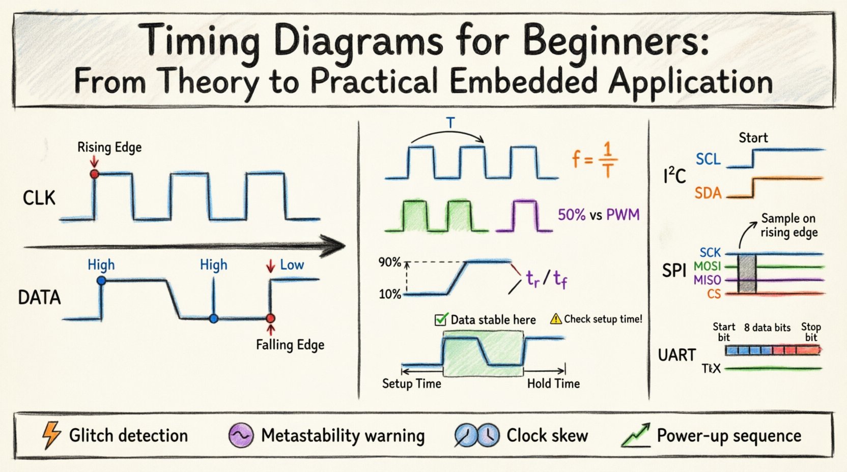
📐 What Is a Timing Diagram?
A timing diagram is a graphical representation of a signal or signals over time. It maps the relationship between different electrical signals within a system. Unlike a logic diagram, which shows connections, a timing diagram shows when events happen.
Key characteristics include:
- Time Axis: The horizontal axis represents time, moving from left to right. It can be linear or non-linear depending on the focus of the analysis.
- Signal Lines: Vertical lines represent individual signals (e.g., Clock, Data, Enable). These are stacked vertically to show relationships.
- Logic Levels: Signals typically toggle between High (Logic 1 / VCC) and Low (Logic 0 / GND).
- Transitions: The change from one level to another is represented by edges (rising or falling).
In embedded systems, timing diagrams ensure that data is sampled at the exact moment it is stable. Without this synchronization, data corruption occurs immediately.
🔑 Core Concepts and Parameters
To read these diagrams effectively, you must understand the specific metrics that define signal integrity. These parameters determine whether a digital circuit functions correctly or fails due to timing violations.
1. Period and Frequency
The period is the time it takes for one complete cycle of a signal to repeat. Frequency is the reciprocal of the period.
- Period (T): Measured in seconds (or nanoseconds, microseconds).
- Frequency (f): Measured in Hertz (Hz). Formula:
f = 1 / T.
In a clock signal, the period dictates the speed at which the processor or peripheral operates. A shorter period means a faster clock speed.
2. Duty Cycle
Duty cycle represents the percentage of one period where the signal is active (High).
- 50% Duty Cycle: The signal is High for half the period and Low for the other half. This is common in standard square waves.
- Non-50% Duty Cycle: Used in specific control applications, such as PWM (Pulse Width Modulation), where the pulse width varies to control power or speed.
3. Rise Time and Fall Time
Signals do not switch instantly. There is a finite time required for voltage to transition between logic levels.
- Rise Time: The time taken to go from Low (10%) to High (90%).
- Fall Time: The time taken to go from High (90%) to Low (10%).
Fast rise and fall times are crucial for high-speed communication. Slow transitions can lead to signal degradation, noise susceptibility, and timing errors.
4. Setup Time and Hold Time
These are the most critical parameters for synchronous digital circuits, particularly when data is captured by a clock edge.
| Parameter | Definition | Why It Matters |
|---|---|---|
| Setup Time (tsu) | The minimum time data must be stable before the clock edge arrives. | Ensures the input latch has enough time to recognize the logic level. |
| Hold Time (th) | The minimum time data must remain stable after the clock edge arrives. | Prevents data from changing while the latch is still closing. |
If the data changes during the setup or hold window, the system may enter a metastable state. This results in unpredictable behavior, where the signal hovers between High and Low for an undefined duration.
📡 Communication Protocols and Timing
Different protocols have unique timing requirements. Understanding the specific diagram for each interface is vital for hardware design and driver development.
1. I2C (Inter-Integrated Circuit)
I2C is a two-wire interface (SCL and SDA) used for short-distance communication between integrated circuits.
- SCL (Serial Clock): Driven by the master. Controls the speed of data transfer.
- SDA (Serial Data): Bidirectional. Data must change only when SCL is Low.
- Start Condition: SDA transitions from High to Low while SCL is High.
- Stop Condition: SDA transitions from Low to High while SCL is High.
In I2C, the timing diagram shows the clock stretching. If a slave device is slow, it can pull the SCL line Low to delay the master until it is ready.
2. SPI (Serial Peripheral Interface)
SPI is a faster, synchronous protocol typically used for flash memory, sensors, and displays.
- SCK (Serial Clock): Generated by the master.
- MOSI (Master Out Slave In): Data from master to slave.
- MISO (Master In Slave Out): Data from slave to master.
- SS/CS (Slave Select): Active low signal to enable a specific device.
SPI timing relies heavily on clock polarity (CPOL) and clock phase (CPHA). The diagram changes based on whether data is sampled on the rising or falling edge of the clock.
3. UART (Universal Asynchronous Receiver-Transmitter)
UART does not use a clock line. Instead, it relies on predefined baud rates (speed) agreed upon by both devices.
- TX/RX Lines: Separate lines for transmit and receive.
- Start Bit: A Low signal indicating the beginning of a frame.
- Data Bits: 5 to 8 bits of actual data.
- Stop Bit: A High signal indicating the end of the frame.
Timing diagrams for UART show the bit period. If the baud rate is 115200, each bit lasts approximately 8.68 microseconds. Deviations in clock accuracy between devices lead to framing errors.
🔍 Reading and Analyzing Timing Diagrams
When you open a datasheet or a logic analyzer trace, you are looking for specific patterns. Here is how to approach analysis systematically.
1. Identify the Clock Source
Locate the regular, periodic signal. This is your reference. All other signals should be analyzed relative to this clock edge. In asynchronous systems, look for the start bit or handshake signals instead.
2. Check Signal Validity Windows
Look at the data lines. Are they stable when the clock samples them? If a data line is toggling exactly when the clock edge arrives, the receiver may read the wrong value. This is often visible as a “glitch” in the middle of a data period.
3. Measure Propagation Delay
Signals take time to travel from one chip to another. If the clock is very fast, the delay might exceed the clock period. Timing diagrams help visualize this skew. If the data arrives late due to wire length, the setup time might be violated.
4. Look for Handshaking
Many protocols use extra lines for flow control (e.g., Busy, ACK, NACK). A timing diagram shows when the master waits for the slave to respond. If the timing doesn’t match the protocol specification, communication fails.
🛠️ Practical Debugging and Troubleshooting
Timing diagrams are the primary tool for debugging hardware issues. When a system fails to initialize or data is corrupted, the diagram tells the story.
1. Identifying Glitches
A glitch is a short pulse that occurs unexpectedly. It might be caused by electrical noise or race conditions in logic gates. In a timing diagram, it appears as a spike that lasts for a few nanoseconds. If a flip-flop captures this spike, it triggers an unwanted state change.
2. Detecting Metastability
Metastability occurs when asynchronous signals are sampled by a synchronous clock. The output voltage hovers in an undefined region between High and Low. On a scope trace, this looks like a slow transition that takes longer than the specified rise time.
3. Analyzing Clock Skew
Skew happens when clock signals reach different parts of the circuit at different times. If the clock reaches the source of the data before the destination, the data might change before it is captured. Timing diagrams allow you to measure the difference in arrival times between clock edges.
4. Verifying Power-Up Sequences
Microcontrollers often require power rails to stabilize in a specific order. A timing diagram can show the voltage ramp-up of VCC and the reset line. If the reset is released too early, the processor might execute garbage code.
⚠️ Common Mistakes in Timing Analysis
Even experienced engineers can overlook details. Here are common pitfalls to avoid.
- Ignoring Voltage Levels: A signal might be “High” logically, but if the voltage is too low (e.g., 2.5V in a 3.3V system), it might not register as a valid 1. Always check voltage thresholds (VIL, VIH).
- Assuming Instantaneous Switching: Real-world signals have rise and fall times. High-speed designs must account for the physical limits of the silicon.
- Overlooking Loading Effects: Connecting too many devices to a bus increases capacitance. This slows down rise and fall times, potentially violating timing constraints.
- Neglecting Temperature: Circuit performance varies with temperature. Timing margins that work at room temperature might fail in extreme heat or cold.
📝 Creating Your Own Timing Diagrams
Documentation is key for team collaboration. When creating diagrams for your own designs, follow these best practices.
- Use Standard Symbols: Stick to industry-standard shapes for edges and levels to ensure clarity.
- Label Time Scales Clearly: Indicate if the scale is linear. If zooming in on a specific event, use a “zoomed” inset view.
- Include Annotations: Add notes explaining critical events, such as “Reset Active” or “Data Valid Window”.
- Specify Conditions: Note the operating conditions (voltage, temperature) under which the timing applies.
| Protocol | Speed | Wires | Typical Use Case |
|---|---|---|---|
| I2C | Low to Medium | 2 | Configuration, Sensors, EEPROM |
| SPI | High | 4 | Flash Memory, Displays, ADCs |
| UART | Low to Medium | 2 | Debug Console, GPS, Bluetooth |
| USB | Very High | 4 | Peripherals, Storage, Power |
🚀 Conclusion on Timing Integrity
Timing diagrams are more than just drawings; they are the verification of signal integrity in embedded systems. By understanding the relationship between time and voltage, engineers can design robust hardware that operates reliably under real-world conditions.
Focus on the parameters that matter most: setup and hold times, rise/fall characteristics, and clock synchronization. When you encounter a failure, trace the signals. Look for the moment the timing breaks down. This systematic approach leads to faster debugging and better product reliability.
Keep your diagrams updated as you change designs. A well-documented timing specification saves countless hours of troubleshooting in the future. Use these visual tools to bridge the gap between theoretical logic and physical reality.