Embedded systems and Internet of Things (IoT) devices rely heavily on precise communication. Without a shared understanding of when data arrives and when signals change state, devices cannot talk to one another effectively. This is where timing diagrams become essential. They serve as the blueprint for digital communication, illustrating the relationship between signals over time. 📈
This guide explores how to read, interpret, and utilize timing diagrams to ensure robust connectivity between microcontrollers, sensors, and communication modules. Whether you are designing a new product or debugging a stubborn connection issue, mastering these visual representations is critical.
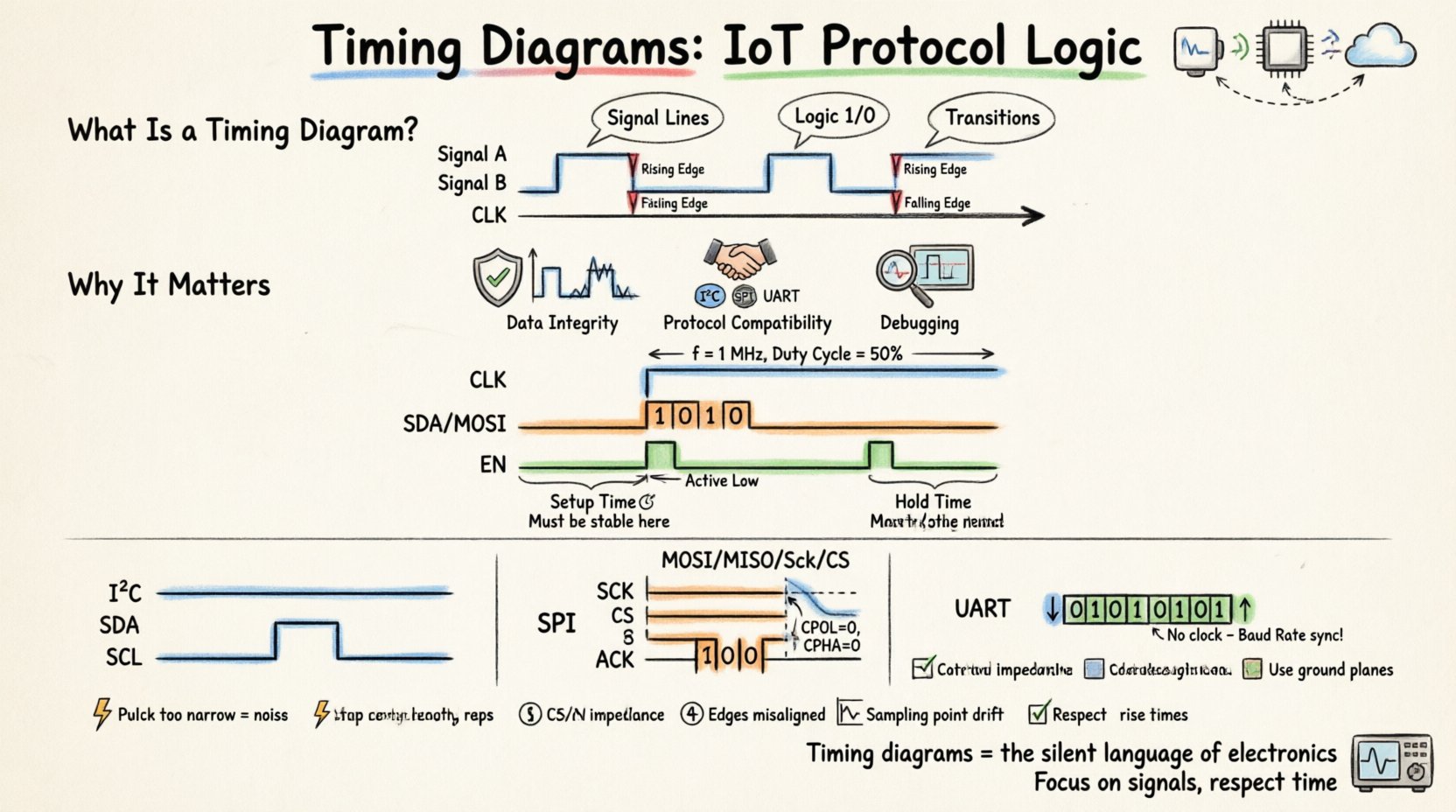
What Exactly Is a Timing Diagram? 📊
A timing diagram is a graphical representation of how digital signals change over time. Unlike logic diagrams that show connections, timing diagrams focus on the when. They plot voltage levels (High/Low) against a time axis, allowing engineers to visualize the sequence of events.
These diagrams are particularly vital in embedded systems because digital logic operates at extremely high speeds. A delay of a few nanoseconds can cause a data packet to be corrupted. By mapping out these moments, engineers can verify that all components adhere to the required specifications.
- Time Axis: Usually runs horizontally, moving from left to right.
- Signal Lines: Horizontal lines represent individual wires or nets.
- Logic Levels: High voltage (Logic 1) and Low voltage (Logic 0).
- Transitions: The moment a signal switches from Low to High or vice versa.
Why Timing Diagrams Matter in IoT 🌐
In the world of IoT, devices often operate with limited power and processing capacity. Efficient communication is not just a luxury; it is a necessity. Timing diagrams help engineers optimize these constraints.
1. Ensuring Data Integrity 🔒
IoT networks often transmit data over noisy environments. Electromagnetic interference (EMI) can flip bits or cause glitches. A timing diagram reveals whether setup and hold times are being met. If a signal changes too close to a clock edge, the receiving device might misinterpret the data. Diagrams help identify these risky windows.
2. Protocol Compatibility 🤝
Different protocols have different rules. I2C requires specific start and stop conditions. SPI relies on clock polarity and phase. Without a timing diagram, it is difficult to verify if a sensor matches the microcontroller’s expectations. These diagrams act as the contract between hardware components.
3. Debugging Communication Errors 🔍
When communication fails, it is rarely random. It is usually a timing violation. By capturing the actual signals on an oscilloscope and overlaying them with the theoretical timing diagram, engineers can pinpoint exactly where the synchronization is lost.
Key Components of a Timing Diagram ⚙️
To read these diagrams effectively, one must understand the standard elements used to construct them. Every diagram, regardless of the protocol, relies on these core concepts.
Clock Signals (CLK) 🕰️
Many IoT protocols are synchronous, meaning they rely on a clock signal to coordinate data transfer. The clock determines the speed of communication.
- Frequency: How many cycles occur per second (Hz, kHz, MHz).
- Duty Cycle: The ratio of High time to the total period.
- Edge: Signals often trigger on the Rising Edge (Low to High) or Falling Edge (High to Low).
Data Lines (SDA, MOSI, TX) 📡
These are the wires carrying the actual information. In a timing diagram, you will see patterns of High and Low states representing binary 1s and 0s.
Control Signals (CS, EN, RD, WR) 🛑
Control lines manage the flow. For example, a Chip Select (CS) line might go Low to enable a specific device on a shared bus. A Read/Write (R/W) line tells the device whether to send data or receive it.
Setup and Hold Times ⏱️
These are critical margins. Setup time is how long before a clock edge the data must be stable. Hold time is how long after the clock edge the data must remain stable. Violating these leads to metastability.
Deep Dive: Common IoT Protocols and Their Timings 🔌
Different communication standards have unique timing requirements. Below, we break down the three most common protocols found in embedded systems.
1. I2C (Inter-Integrated Circuit) 🧩
I2C is popular for connecting low-speed peripherals like sensors. It uses two lines: SDA (Data) and SCL (Clock).
| Feature | Timing Characteristic |
|---|---|
| Start Condition | SDA transitions High to Low while SCL is High. |
| Stop Condition | SDA transitions Low to High while SCL is High. |
| Data Validity | Data must be stable while SCL is High. Changes only when SCL is Low. |
| Acknowledge (ACK) | Receiver pulls SDA Low during the 9th clock pulse. |
The Start condition signals the beginning of a transaction. The Stop condition signals the end. Crucially, the data line is only allowed to change state when the clock is Low. If a device changes data while the clock is High, it mimics a Start or Stop condition, causing confusion.
2. SPI (Serial Peripheral Interface) 🚀
SPI is faster than I2C and is used for high-bandwidth devices like SD cards or displays. It typically uses four lines: MOSI, MISO, SCK, and CS.
- Clock Polarity (CPOL): Defines the idle state of the clock. Is it High or Low?
- Clock Phase (CPHA): Defines when data is sampled. At the first or second clock edge?
There are four modes of operation in SPI, defined by the combination of CPOL and CPHA. A timing diagram must clearly indicate the idle state and the active edges. Unlike I2C, SPI does not have built-in acknowledge bits; the master simply expects data back.
3. UART (Universal Asynchronous Receiver-Transmitter) 📟
UART is asynchronous, meaning it does not use a shared clock. Instead, it relies on a pre-agreed Baud Rate.
- Idle State: Typically High.
- Start Bit: A transition from High to Low indicates the start of a byte.
- Stop Bit: A transition back to High marks the end.
Timing is critical here because there is no clock to synchronize the two devices. If the Baud Rate is off by even a small percentage, the receiving end will sample the bits at the wrong time, resulting in errors. The timing diagram shows the pulse width of the Start and Stop bits relative to the data bits.
How to Read a Timing Diagram Step-by-Step 🧐
When faced with a new protocol specification, follow this systematic approach to decode the timing diagram.
- Identify the Clock: Find the periodic signal. Determine its frequency and duty cycle.
- Determine Active Edges: Look for arrows or notes indicating which edge triggers the action. Is it Rising or Falling?
- Check Data Validity Windows: Look for the shaded regions where data is stable. This is where the receiver is allowed to read the value.
- Locate Control Signals: Identify Chip Select, Reset, or Enable lines. Note when they go active relative to the clock.
- Verify Margins: Check for setup and hold time annotations. Ensure the physical implementation can meet these requirements.
Troubleshooting with Timing Diagrams 🛠️
When a system fails to communicate, the timing diagram is your primary diagnostic tool. Here are common failure modes and how the diagram helps identify them.
1. Glitches and Noise ⚡
Short spikes on a signal line can be interpreted as valid edges. A timing diagram helps distinguish between a genuine signal transition and electrical noise. If a pulse is narrower than the minimum specification, it is likely noise.
2. Clock Skew 🏁
Clock skew occurs when the clock signal arrives at different devices at different times. In a timing diagram, this looks like a shift in the clock edge relative to the data edge. If the skew exceeds the timing budget, the system will fail.
3. Baud Rate Mismatch (UART) 📉
If the transmitter and receiver are not perfectly synchronized, the sampling points drift. Over time, the receiver might sample the next bit instead of the current one. The timing diagram visualizes this drift, showing the accumulation of error bits.
4. Pull-up Resistor Issues (I2C) 🧱
I2C lines are open-drain and require pull-up resistors. If the resistance is too high, the signal rises slowly. A timing diagram will show a slow rise time, potentially causing the signal to not reach the High threshold before the clock edge arrives.
Best Practices for Designing Reliable Timings 📝
Designing for timing success requires attention to detail from the schematic stage to the PCB layout. Follow these guidelines to minimize issues.
- Match Trace Lengths: For parallel buses, keep traces equal length to avoid skew. For serial buses, ensure the clock path is clean.
- Manage Impedance: Use controlled impedance traces to prevent signal reflections, which distort timing.
- Decoupling Capacitors: Place capacitors near power pins to ensure stable voltage during switching, which prevents timing jitter.
- Respect Rise Times: Ensure the driver can switch fast enough to meet the protocol’s minimum rise/fall time requirements.
- Use Ground Planes: A solid ground plane reduces noise and provides a stable reference for voltage levels.
Advanced Considerations: Latency and Throughput 🚀
Timing diagrams are not just about correctness; they are about performance. Understanding the timing allows you to calculate latency and throughput.
Calculating Throughput
By analyzing the clock frequency and the number of bits per cycle in the diagram, you can determine the maximum data rate. For example, if a clock runs at 1 MHz and one bit is sent per cycle, the throughput is 1 Mbps.
Minimizing Latency
Latency is the time from when data is ready to when it is received. Timing diagrams show the idle periods between transactions. Reducing these idle periods (e.g., by optimizing Start/Stop conditions in I2C) can significantly improve system responsiveness.
The Role of Logic Analyzers 🔬
While timing diagrams are theoretical, logic analyzers provide the empirical data. These tools capture the actual voltage levels on multiple channels simultaneously and display them as a timing diagram.
When debugging, you capture the signal, then compare the captured waveform against the specification diagram. Any deviation is a clue. Modern tools allow you to decode the binary data into ASCII or Hex, making the analysis much faster.
Conclusion: The Backbone of Embedded Communication 🔗
Timing diagrams are the silent language of electronics. They do not shout, but they dictate the rules of engagement for every digital interaction. For IoT engineers, understanding these diagrams is not optional; it is fundamental.
By mastering the visual logic of clock edges, data validity windows, and control signals, you ensure that your devices communicate reliably in the real world. Whether dealing with the low-speed constraints of I2C or the high-speed demands of SPI, the timing diagram remains the constant truth.
As technology evolves, new protocols will emerge with tighter timing requirements. The ability to read and interpret these diagrams will remain a core competency for anyone building connected systems. Focus on the signals, respect the time, and your designs will succeed.