Designing digital systems requires precision. You create a timing diagram, simulate the behavior, and expect the physical hardware to follow the blueprint exactly. However, in practice, discrepancies often emerge. Signals arrive late, pulses vanish, or data appears corrupted. When your timing diagram does not match hardware behavior, it indicates a gap between the theoretical model and physical reality. This guide provides a structured approach to diagnosing and resolving these mismatches without relying on hype or unverified shortcuts.
The divergence between simulation and silicon is a common engineering challenge. It often stems from parasitic effects, clock distribution issues, or incorrect assumptions about signal propagation. To bridge this gap, you need a methodical debugging process. This article covers the root causes of timing discrepancies, diagnostic techniques, and strategies to align your design with actual hardware performance.
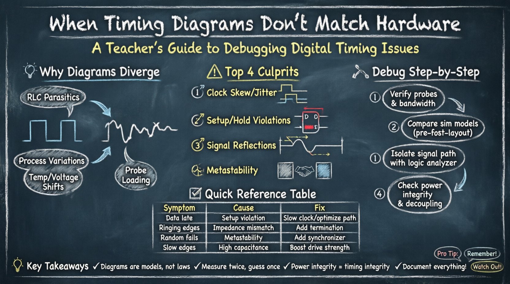
🧐 Why Timing Diagrams Diverge from Reality 📉
A timing diagram represents an idealized view of signal transitions over time. It assumes zero delay, perfect edges, and infinite bandwidth. Hardware, however, operates under physical constraints. Resistance, capacitance, and inductance (RLC) affect every trace on a board. When the diagram fails to account for these factors, the hardware behaves differently.
- Ideal vs. Real Models: Simulation tools often use abstract models that simplify propagation delays. Physical boards introduce variance based on trace length and material.
- Process Variations: Manufacturing tolerances mean transistors switch at slightly different speeds across a single chip.
- Environmental Factors: Temperature and voltage fluctuations alter the speed of logic gates.
- Measurement Artifacts: Probing hardware introduces load, which can slow down signals that were previously fast enough.
Understanding these distinctions is the first step. If you treat the timing diagram as an absolute law rather than a prediction, you will struggle to find the actual faults. The goal is to identify where the model breaks down.
⏱ Common Causes of Timing Discrepancies ⚠️
Several specific mechanisms typically cause the mismatch between your design expectations and physical execution. Identifying the culprit requires isolating variables.
1. Clock Skew and Jitter
Clock distribution is the backbone of synchronous logic. In a diagram, the clock edge is often a vertical line. On a board, the clock edge spreads out. Clock skew occurs when the clock signal arrives at different registers at different times. Jitter refers to the variation in the clock period.
- Global Skew: The clock path to one register is significantly longer than to another.
- Local Skew: Differences in load capacitance on adjacent clock nets.
- Impact: If skew exceeds the slack budget, setup and hold violations occur, leading to metastability.
2. Setup and Hold Time Violations
Flip-flops require data to be stable before and after the clock edge. The timing diagram often assumes perfect stability. Hardware reveals the truth.
- Setup Time Violation: Data arrives too late for the next clock cycle. The logic fails to capture the value correctly.
- Hold Time Violation: Data changes too soon after the clock edge. The current value is overwritten by the new input before it settles.
- Diagnosis: Check the propagation delay of combinational logic against the clock period.
3. Signal Integrity and Reflections
High-speed signals behave like transmission lines. If the impedance is not matched, reflections occur. The timing diagram shows a clean transition. The oscilloscope shows ringing or overshoot.
- Impedance Mismatch: Trace width and dielectric thickness affect characteristic impedance.
- Termination: Without proper termination, signals bounce between the driver and receiver.
- Crosstalk: Aggressive switching on adjacent nets induces noise, altering the perceived timing of the victim net.
4. Metastability in Asynchronous Interfaces
When crossing clock domains, data may arrive at an invalid time. The timing diagram might show a handshake protocol. The hardware might hang or produce garbage data.
- Synchronizers: Use multi-flop synchronizers to reduce the probability of metastability.
- Handshakes: Ensure request/acknowledge signals have sufficient setup time relative to the destination clock.
- Timing Margins: Asynchronous signals require careful margin analysis to prevent corruption.
🔍 Diagnostic Methodology: Step-by-Step Analysis 🔬
When a mismatch occurs, do not guess. Follow a structured debugging path. This ensures you address the root cause rather than symptoms.
Step 1: Verify the Measurement Setup
Before blaming the design, confirm the measurement chain. Probes have capacitance. A high-impedance probe can load the circuit.
- Probe Compensation: Ensure probes are properly compensated for the frequency range.
- Ground Leads: Long ground leads act as antennas and introduce inductance. Use ground springs for high-speed signals.
- Bandwidth: Ensure the oscilloscope bandwidth exceeds the signal frequency by at least 5x.
Step 2: Compare Simulation Models
Review the constraints used in the simulation environment. Are they matching the physical layout?
- Library Models: Check if the simulation uses typical, worst-case, or best-case models.
- Parasitics: Did you extract post-layout parasitics? Pre-layout simulation ignores trace resistance and capacitance.
- Constraints: Verify that the clock definitions in the constraint file match the actual clock source.
Step 3: Isolate the Signal Path
Identify which specific signals are causing the issue. Use a logic analyzer or oscilloscope to capture the waveform.
- Toggle Rate: Are the signals toggling at the expected frequency?
- Rise/Fall Times: Measure the edge steepness. Slow edges indicate high load or drive strength issues.
- Glitches: Look for transient pulses that might trigger logic incorrectly.
Step 4: Analyze Power and Ground
Power integrity is often overlooked. Voltage droop affects switching speed.
- Decoupling: Ensure capacitors are placed close to power pins.
- Ground Bounce: Switching currents can lift the ground reference, altering logic thresholds.
- Supply Noise: Check for noise coupling from switching regulators into sensitive analog or digital sections.
📊 Common Timing Errors and Solutions Table 🛠
Use this reference table to quickly identify potential issues based on observed symptoms.
| Observed Symptom | Likely Cause | Verification Method | Recommended Fix |
|---|---|---|---|
| Data arrives late | Setup Time Violation | Check propagation delay vs clock period | Slow down clock or optimize logic path |
| Data changes too early | Hold Time Violation | Check minimum delay of combinational logic | Add delay buffers or redesign path |
| Signal edges are slow | High Capacitive Load | Measure rise time with oscilloscope | Reduce trace length or increase drive strength |
| Ringing on edges | Impedance Mismatch | Inspect waveform for overshoot | Apply series termination resistor |
| Random failures | Metastability | Check asynchronous handshakes | Add synchronizer stages |
| Periodic errors | Clock Jitter | Analyze clock spectrum | Improve PLL configuration or power filtering |
| Intermittent glitches | Crosstalk | Check adjacent net activity | Increase spacing or add shielding |
| Logic stuck low/high | Power/Ground Issue | Monitor supply voltage rails | Improve decoupling or ground plane |
🧩 Advanced Scenarios and Nuances 🔎
Beyond the basics, complex systems introduce specific challenges that require deeper analysis.
Multi-Domain Clocking
Systems often run at multiple frequencies. Synchronizing data between 100MHz and 200MHz domains is not straightforward. The timing diagram might show a simple arrow. Hardware requires a handshake protocol.
- FIFOs: Use asynchronous FIFOs for large data blocks.
- Gray Codes: Use Gray codes for pointer crossing to ensure only one bit changes.
- Phase Alignment: If clocks are related, ensure phase alignment to avoid sampling at the wrong edge.
Temperature and Voltage Corners
Simulation usually runs at nominal conditions. Hardware operates in a range. A design that works at 25°C might fail at 85°C.
- Slow-Slow Corner: Worst-case for setup time (slowest transistors).
- Fast-Fast Corner: Worst-case for hold time (fastest transistors).
- Validation: Test hardware across the full operating temperature and voltage range.
Probe Loading Effects
This is a frequent source of false negatives. When you connect a probe, you add capacitance. A node that toggles in simulation might slow down in reality because the probe loads it.
- Active Probes: Use active probes with lower capacitance for high-speed nodes.
- Non-Intrusive: Where possible, use internal debug logic instead of physical probes.
- Estimation: Calculate the added capacitance and check if it exceeds the driver capability.
🛡 Prevention Strategies for Future Designs 🛡
Once you fix the current issue, apply these strategies to prevent recurrence.
1. Early Timing Closure
Do not wait until the board is built to check timing. Run static timing analysis (STA) early in the design flow.
- Incremental Updates: Update constraints as the design evolves.
- Report Analysis: Review timing reports for critical paths regularly.
- Constraint Files: Maintain accurate SDC or equivalent constraint files.
2. Robust PCB Layout
The physical design dictates the timing performance.
- Layer Stackup: Define controlled impedance layers.
- Length Matching: Match lengths for differential pairs and buses.
- Via Minimization: Reduce vias on high-speed lines to minimize discontinuity.
3. Design for Testability
Build features that allow you to observe internal states.
- Scan Chains: Use scan chains to shift out state for debugging.
- Loopbacks: Enable loopback modes for signal integrity testing.
- Debug Ports: Expose select signals to external pins for logic analysis.
4. Documentation
Maintain clear documentation of the timing assumptions.
- Timing Reports: Archive reports for every version.
- Constraint Notes: Document why specific constraints were chosen.
- Hardware Notes: Record the actual behavior of the prototype for future reference.
🔄 Iterative Debugging Process 🔄
Debugging is rarely linear. You will likely cycle through these steps multiple times.
- Define the Symptom: Be specific. “Data is wrong” is not enough. “Bit 3 is inverted on the rising edge” is actionable.
- Hypothesize: Form a theory based on the timing diagram and hardware behavior.
- Test: Change one variable at a time. Modify constraints, add delays, or change probe points.
- Measure: Capture the new behavior. Compare it to the hypothesis.
- Refine: If the hypothesis is wrong, discard it and form a new one.
This iterative loop prevents you from getting stuck. It forces objective observation over confirmation bias. Often, the problem is not in the logic, but in the environment or the measurement tool.
📝 Summary of Key Takeaways 📝
- Timing diagrams are models, not laws. They simplify reality and may omit parasitics.
- Physical effects matter. Trace length, impedance, and load capacitance change signal behavior.
- Measurement quality is critical. Probes can alter the circuit they are measuring.
- Static Timing Analysis is essential. It predicts violations before hardware is fabricated.
- Isolate variables. Change one thing at a time to identify the root cause.
- Power integrity is part of timing. Voltage droop affects switching speed.
- Document everything. Knowledge gained during debugging is valuable for the next project.
Resolving a timing mismatch requires patience and technical rigor. There are no magic tools that fix physical reality. However, by understanding the physics of signal propagation and adhering to a disciplined debugging process, you can align your design with hardware expectations. This alignment ensures reliability and performance in the final product.
Continue to refine your understanding of signal integrity and timing closure. As systems become faster and denser, the margin for error shrinks. A deep grasp of these troubleshooting techniques will keep your designs robust against the complexities of modern electronics.