Creating accurate timing diagrams is a foundational skill for anyone working in embedded systems and firmware development. These diagrams act as the contractual agreement between hardware and software. When the timing is misaligned, the system fails, often in subtle and difficult-to-diagnose ways. A timing diagram is not merely a drawing; it is a representation of physical reality governed by electrical properties, clock speeds, and signal propagation delays.
Firmware engineers often underestimate the complexity of hardware interfaces. They may assume that a signal transition happens instantaneously or that a bus protocol is strictly synchronous. However, the physical world introduces latency, noise, and metastability. Ignoring these factors leads to race conditions, data corruption, and intermittent failures that can plague a product for months. This guide explores the most frequent errors made when interpreting or creating timing diagrams for firmware logic and provides concrete strategies to ensure robustness.
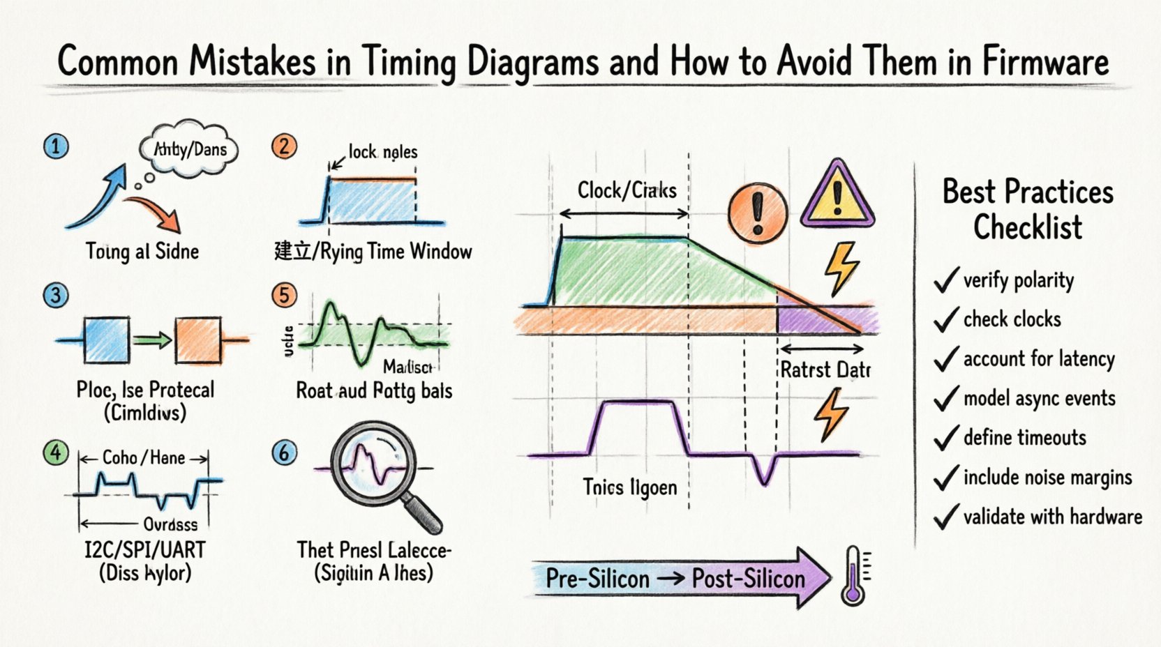
⏱️ Mistake 1: Misinterpreting Edge Triggers and Signal Levels 📉
One of the most common pitfalls is assuming that every transition on a bus line is meaningful or that the polarity is intuitive. In hardware design, signals can be active-high or active-low. A firmware developer might write code expecting a rising edge to trigger an interrupt, while the hardware schematic indicates a falling edge is required for the operation.
Without a clear timing diagram, the firmware might wait for a condition that never arrives, or worse, trigger on noise spikes. This is particularly dangerous in high-speed interfaces where glitches can mimic valid data transitions.
- The Error: Assuming a signal is edge-triggered when it is actually level-sensitive, or vice versa.
- The Consequence: The interrupt service routine (ISR) fires repeatedly on a single event, or fails to fire entirely during normal operation.
- The Solution: Always verify the signal polarity against the hardware specification. Look for inversion bubbles on the schematic. If the diagram shows a low pulse for activation, ensure the firmware checks for a logic zero, not a transition.
- The Risk: Race conditions where the firmware misses a narrow pulse if the sampling rate is too slow.
Furthermore, consider the distinction between setup and hold time in the context of edge detection. A signal might appear stable on an oscilloscope trace, but if the clock edge arrives too close to the data transition, the receiving flip-flop may enter a metastable state. The firmware logic does not see a clean 0 or 1; it sees a voltage fluctuating in the undefined region. This leads to unpredictable behavior where the same code executes differently under different thermal or voltage conditions.
📏 Mistake 2: Ignoring Setup and Hold Time Violations 📐
Setup and hold times are critical constraints defined by the hardware manufacturer. Setup time is the minimum duration data must be stable before the clock edge. Hold time is the minimum duration data must remain stable after the clock edge. Firmware developers often treat these as soft constraints, assuming the system will work as long as the code is “fast enough.”
This is a dangerous assumption. If the timing diagram does not explicitly account for these windows, the firmware might attempt to read data that is still changing. This results in sampling errors that are difficult to reproduce in a lab environment.
| Timing Parameter | Definition | Common Firmware Error | Impact |
|---|---|---|---|
| Setup Time | Data stable before clock edge | Reading data too early | Invalid data captured |
| Hold Time | Data stable after clock edge | Changing data too soon | Glitches on output line |
| Clock-to-Q Delay | Time for output to change after clock | Assuming instant output | Next stage receives old data |
To avoid this, firmware must be written with the worst-case timing margins in mind. This often means introducing small software delays or polling loops to ensure the signal has settled before reading. In synchronous designs, the firmware must align its read operations with the rising or falling edge of the external clock, not the internal processor clock. If the internal clock is faster than the external interface, a simple read operation might miss the window entirely.
🔄 Mistake 3: Clock Domain Crossing Issues ⏲️
Embedded systems often operate with multiple clock domains. For example, a microcontroller might run at 48 MHz while an external sensor communicates via a 10 MHz SPI bus. When firmware moves data between these two domains, timing diagrams must account for the phase relationship between the clocks. Without proper synchronization, data can be lost or corrupted.
This is known as a Clock Domain Crossing (CDC) issue. If the firmware samples data from the slow domain using the fast domain’s clock without synchronization logic, metastability can occur. The data might be sampled at the wrong phase, leading to bit flips.
- Asynchronous Sampling: Reading a signal that changes at an unpredictable rate relative to the sampling clock.
- Metastability: The output of a flip-flop becomes undefined, oscillating between 0 and 1 for an indeterminate time.
- Loss of Data: If the pulse width of the signal is shorter than the sampling period of the faster clock, the event is skipped.
To mitigate this, firmware should implement synchronization registers. This involves registering the input signal twice or three times before using it in logic. This delays the signal by a few clock cycles but ensures that metastability has resolved before the data is processed. In timing diagrams, this delay must be explicitly modeled to ensure the downstream logic has time to react.
Additionally, consider the skew between clock signals. If the clock tree is not balanced, the clock edge might arrive at different points in the chip at different times. This is critical in high-speed parallel interfaces. A timing diagram that assumes all bits of a data bus arrive simultaneously is often incorrect. Skew can cause the most significant bit (MSB) to be sampled before the least significant bit (LSB), leading to misalignment errors.
📡 Mistake 4: Oversimplifying Bus Protocols 🛠️
Standard protocols like I2C, SPI, and UART have well-defined timing requirements. However, firmware engineers often generalize these requirements. For instance, I2C has a specific clock stretching feature where the slave device holds the clock line low to slow down the master. If the firmware does not account for this, it may timeout the transaction prematurely.
Similarly, in SPI, the mode (CPOL and CPHA) determines when the data is sampled relative to the clock edge. There are four valid modes. Choosing the wrong mode in software results in a reversal of data bits or sampling on the wrong edge.
| Protocol | Key Timing Requirement | Typical Firmware Oversight | Correction |
|---|---|---|---|
| I2C | Start/Stop conditions & Clock Stretching | Ignoring SCL hold time | Implement wait loops for SCL low |
| SPI | Clock Polarity & Phase | Defaulting to Mode 0 | Match hardware CPHA/CPOL config |
| UART | Baud Rate Accuracy & Sampling | Assuming perfect timing | Calculate exact baud rate divisor |
Another common error involves the termination of transactions. In many bus protocols, the master initiates the communication, but the slave signals completion. If the firmware assumes the transaction ends after a specific number of bytes without checking the acknowledgment lines, it may leave the bus in a hung state. This can block other devices from communicating on the same bus.
Timing diagrams for bus protocols must show the acknowledgment bits, the idle periods between bytes, and the recovery times required between transactions. Skipping these details in the diagram leads to firmware that works in a vacuum but fails when multiple peripherals are connected.
📉 Mistake 5: Neglecting Signal Integrity & Noise 🌩️
A timing diagram drawn in a perfect world often looks different on a noisy PCB. Electromagnetic interference (EMI), crosstalk, and power supply ripple can distort signals. A clean square wave in the schematic might look like a noisy ramp on the actual board.
Firmware that relies on precise voltage thresholds may fail if the noise floor is too high. For example, a digital input pin might float near the logic threshold. Without hysteresis or proper filtering, the firmware might read a high, then a low, then a high again in rapid succession, triggering false interrupts.
- Debouncing: Mechanical switches and relay contacts bounce. Firmware must implement software debouncing or wait for signal stability.
- Ground Bounce: When multiple outputs switch simultaneously, the ground reference can shift. This changes the effective voltage levels seen by inputs.
- Reflections: On long traces, signal reflections can cause ringing. This creates multiple false edges that the firmware might interpret as data.
To address this, timing diagrams should include noise margins. This defines the range of voltage where the signal is considered valid. Firmware should sample multiple times and take the majority vote (voting logic) to filter out transient glitches. In high-noise environments, using differential signaling (like RS-485) is preferable, as the timing logic focuses on the difference between two lines rather than a single voltage level.
When debugging signal integrity issues, an oscilloscope is the primary tool. It allows you to see the actual waveform, including overshoot and undershoot. If the timing diagram does not account for these physical characteristics, the firmware will be brittle. A robust design assumes that signals will degrade over time due to aging components or environmental changes.
🔍 Mistake 6: Debugging Without Context 🔬
When a system fails, the first reaction is often to add print statements or toggle GPIO pins to debug. This is known as “instrumentation debugging.” However, adding instrumentation changes the timing of the system. The act of writing to a buffer or toggling a pin takes clock cycles. This can alter the timing of the very bug you are trying to find.
This is a classic Heisenbug: the bug disappears when you try to observe it. The timing diagram captured during debug may not reflect the timing during production. To avoid this, use hardware debuggers that can capture logic analyzer traces without impacting the system clock. This ensures the timing diagram remains accurate to the production environment.
Additionally, do not rely on software delays (like delay_ms) for critical timing. These are often inaccurate due to interrupts, cache misses, or variable compiler optimization. Hardware timers and capture/compare units are far more reliable for generating precise waveforms.
✅ Best Practices Checklist for Timing Accuracy ✅
To ensure your firmware interacts correctly with hardware, follow this checklist when reviewing or creating timing diagrams.
- Verify Signal Polarity: Check if active signals are high or low.
- Check Clock Frequencies: Ensure the firmware clock matches the hardware interface clock.
- Account for Latency: Include processing time in the total transaction time.
- Model Asynchronous Events: Clearly mark which signals are asynchronous to the main clock.
- Define Timeout Values: Set timeouts based on the slowest expected response, not the fastest.
- Include Noise Margins: Define acceptable voltage ranges for logic levels.
- Validate with Hardware: Always verify timing diagrams with a real oscilloscope, not just simulation.
- Document State Changes: Clearly mark the state of the bus before and after a transaction.
🔧 Pre-Silicon vs Post-Silicon Considerations ⚙️
The approach to timing diagrams changes depending on the stage of development. In pre-silicon (simulation), you have access to ideal models. You can assume zero propagation delay and perfect clocks. In post-silicon (hardware), you must account for parasitic capacitance and inductance.
When moving from simulation to hardware, the firmware team must be prepared for timing drift. A timing diagram that worked in the simulator might fail on the board due to trace length differences. It is crucial to build margin into the firmware. If the hardware spec says 10 microseconds, the firmware should expect up to 15 microseconds in worst-case scenarios.
Furthermore, consider temperature. Silicon speed varies with temperature. At high temperatures, transistors switch slower. At low temperatures, they switch faster. A timing diagram must consider the full operating temperature range of the device. If the firmware is too tight at room temperature, it may fail in a hot environment.
📝 Final Considerations for Robust Firmware 🏁
Timing diagrams are not static documents. They evolve as the hardware and software interact. A good firmware engineer treats the timing diagram as a living contract. It must be updated whenever a hardware revision occurs or a new peripheral is added. Regular review of these diagrams with the hardware team is essential.
The goal is not just to make the code work, but to make it work reliably under all conditions. This requires a deep understanding of the physical constraints of the system. By avoiding the common mistakes outlined above, you can build firmware that is resilient, predictable, and maintainable. Focus on the margins, respect the clocks, and always verify with real hardware measurements. This discipline separates production-ready code from prototypes that only work in the lab.