Embedded development relies heavily on the synchronization between software instructions and physical hardware signals. When firmware interacts with sensors, displays, or communication buses, precision is non-negotiable. A timing diagram serves as the blueprint for this interaction, visually mapping out how signals behave over time. This guide provides a structured approach to creating these diagrams without relying on specific proprietary tools, focusing on the core principles that ensure your firmware functions correctly within its hardware environment.
Whether you are debugging a stubborn I2C communication issue or defining a new interface for a microcontroller, understanding the temporal relationship between signals is critical. This document breaks down the essential elements, the step-by-step creation process, and the common pitfalls to avoid. By the end of this reading, you will have a solid foundation for documenting signal behavior that bridges the gap between code logic and electrical reality.
Understanding the Fundamentals of Signal Timing 🧩
A timing diagram is a graphical representation of how electrical signals change state over time. In the context of firmware, these signals represent the physical lines connecting your processor to peripheral devices. The horizontal axis represents time, moving from left to right. The vertical axis represents the logic level or voltage state of the signal.
- Time Axis: This is the reference for when events occur. In firmware, this often correlates to clock cycles, instruction cycles, or absolute time in milliseconds.
- Signal Axis: Each horizontal line represents a specific wire or net. Labels must clearly identify the function, such as
CLK,DATA, orCS(Chip Select). - Logic Levels: Signals are typically binary. High voltage (e.g., 3.3V) represents a logical 1, and Low voltage (e.g., 0V) represents a logical 0. Some protocols use High-Z (High Impedance) states where the pin is electrically disconnected.
Accuracy in these diagrams is vital. A misaligned edge in a diagram can lead to a firmware driver that writes data to the wrong moment, causing corruption or hardware lockups. The diagram acts as a contract between the hardware designer and the firmware engineer.
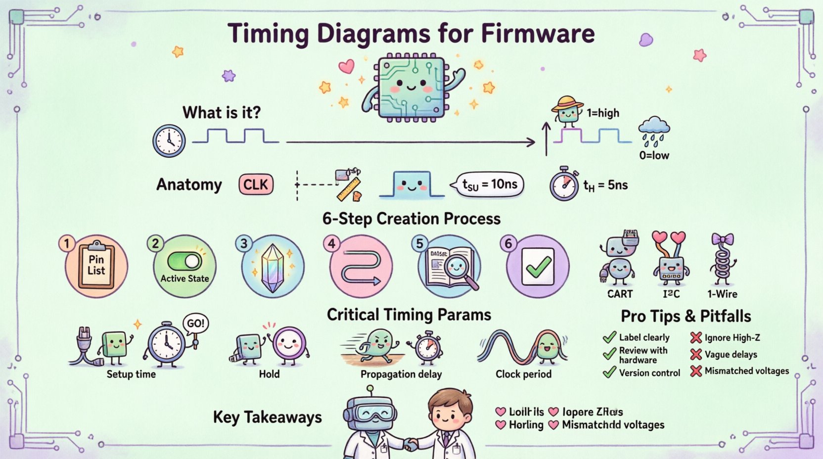
Anatomy of a Professional Timing Diagram 📊
To create a document that is useful for debugging and documentation, you must adhere to specific structural standards. A disorganized diagram is difficult to read and prone to misinterpretation. Below are the core components required for a clear representation.
- Signal Names: Every line must have a unique label. Avoid generic names like
Signal_1. Use standard abbreviations likeMOSIorRST. - Time Markers: Vertical dashed lines often indicate specific points of interest. These help align events across multiple signals, such as a clock edge triggering a data read.
- Waveforms: Signals can be square, triangular, or sinusoidal. For digital firmware, square waves are the norm. Sharp transitions indicate clean switching, while rounded edges may suggest noise or bandwidth limitations.
- Annotations: Text notes explain specific conditions. For example, noting that a line is active low means the signal performs its function when the voltage is low.
- Parameters: Specific time values (like
tsufor setup time) should be labeled on the diagram to define the constraints.
When drawing these by hand or using a generic canvas, consistency is key. Ensure all vertical transitions align perfectly with the time markers you define. Misalignment creates ambiguity.
Step-by-Step Process for Creation 📝
Creating a timing diagram is a systematic process. It begins with gathering requirements and ends with a review for clarity. Follow these steps to ensure the diagram accurately reflects the intended behavior.
- Identify the Signals: List every pin involved in the interaction. This includes data lines, control lines, and clock sources.
- Determine the Active State: Decide which voltage level triggers the action. Is the Chip Select active high or active low? This must be clear in the diagram.
- Define the Clock Source: Identify where the timing originates. Is it internal to the microcontroller or provided by an external crystal?
- Map the Sequence: Draw the sequence of events. Start with the trigger, followed by the data transfer, and end with the completion signal.
- Label Timing Parameters: Add the specific time values required by the datasheet. Do not guess these values.
- Review Against Hardware: Cross-reference the diagram with the schematic and the datasheet to ensure electrical compatibility.
It is often helpful to sketch the worst-case scenario. If your firmware works in the worst-case timing conditions, it will work in all conditions.
Common Communication Protocols and Their Diagrams 🔌
Different hardware interfaces have distinct timing requirements. Understanding the standard patterns for these protocols allows you to quickly identify issues when the diagram does not match the observed behavior. Below are examples of how these protocols typically appear.
| Protocol | Key Signals | Timing Characteristic | Typical Use Case |
|---|---|---|---|
| UART | TX, RX, GND | Asynchronous, Start/Stop bits | Console output, Serial debugging |
| I2C | SDA, SCL | Synchronous, Open Drain | Sensors, EEPROMs |
| SPI | SCK, MOSI, MISO, CS | Synchronous, Full Duplex | Flash memory, Displays |
| 1-Wire | Data, GND | Single line, Time-slotted | Temperature sensors |
For I2C, the timing diagram must show the Start condition (SDA goes low while SCL is high) and the Stop condition (SDA goes high while SCL is high). The Acknowledge (ACK) bit is also critical and should be marked clearly.
For SPI, the diagram must indicate the polarity of the clock. Does the data change on the rising or falling edge? This is often defined by the clock phase setting in the firmware configuration register.
Critical Timing Parameters Explained ⏱️
When firmware engineers read a timing diagram, they look for specific constraints that dictate how the code must be written. Ignoring these parameters is a common cause of intermittent bugs.
Setup Time (tsu)
Setup time is the minimum amount of time a data signal must be stable before a clock edge occurs. If the firmware changes the data too quickly before the clock triggers the read, the data will be sampled incorrectly. In code, this might mean delaying the toggling of a control pin or ensuring interrupts are disabled during critical data setup.
Hold Time (th)
Hold time is the minimum amount of time the data signal must remain stable after the clock edge. If the signal changes too soon after the clock, the receiving device may not latch the value. This is crucial for high-speed interfaces where the processor might be faster than the peripheral.
Propagation Delay (tpd)
This is the time it takes for a signal to travel from the input of a component to its output. In firmware, this affects how quickly a response is expected after a command is sent. If the firmware polls a status register too early, it may read stale data.
Clock Frequency and Period
The clock period is the inverse of the frequency. If the clock is 1 MHz, the period is 1 microsecond. All timing parameters must be compared against this period. A setup time of 500ns is acceptable for a 1MHz clock but might fail for a 100MHz clock.
Firmware Considerations and Code Timing 🖥️
A timing diagram is not just about hardware; it is also about how the compiler translates your code into machine instructions. The diagram must account for the execution time of the firmware logic itself.
- Interrupt Latency: When an interrupt occurs, the processor pauses the current task to run an Interrupt Service Routine (ISR). The time taken to enter the ISR must be factored into the timing budget. If the ISR takes too long, you might miss the next clock edge.
- Polling Loops: If you poll a status bit in a loop, the time it takes to execute the loop determines how fast you can react. A tight loop consumes less time than a loop with complex calculations.
- Compiler Optimization: Compilers may reorder instructions or inline functions. This can change the exact timing of pin toggles. For critical timing, you may need to use assembly code or specific compiler directives to prevent optimization from altering the sequence.
- Bus Arbitration: If multiple masters control the bus, the timing diagram must show the arbitration process. The firmware must know how long to wait for the bus to become free.
Common Pitfalls and Best Practices ⚠️
Even experienced engineers make mistakes when drafting these diagrams. Being aware of common errors helps you create more robust documentation.
- Ignoring High-Z States: Many diagrams only show High and Low. However, many interfaces use High-Z (floating) states. If a pin is released by the master, it becomes High-Z. The diagram should indicate this, as it affects how pull-up resistors behave.
- Mismatched Logic Levels: Ensure that the voltage levels in the diagram match the datasheet. Some chips operate at 1.8V while others operate at 3.3V. Mixing these without a level shifter can damage hardware.
- Overlooking Glitches: Short pulses, known as glitches, can sometimes occur during transitions. If your firmware samples during a glitch, it may interpret a transient state as a valid command.
- Vague Annotations: Avoid labels like “wait” or “delay.” Use specific time values like “10µs” or “2 clock cycles.” Vague labels lead to guessing during implementation.
- Lack of Revision Control: Timing diagrams evolve as hardware changes. Always include a version number and a date on the document. This prevents the firmware team from working off an outdated specification.
Collaboration with Hardware Teams 🤝
Timing diagrams are a shared language between firmware and hardware engineers. Effective collaboration ensures that both sides agree on the interface behavior before coding begins.
- Early Review: Share the draft diagram with the hardware team before writing any driver code. They can verify that the electrical constraints are feasible with the selected components.
- Clarify Handshakes: Define exactly how a device signals it is ready. Is it a dedicated line, or is it a timeout mechanism? The diagram should explicitly show the handshake sequence.
- Discuss Power States: Devices may enter sleep modes that affect their timing. The diagram should indicate if timing parameters change when the device is active versus standby.
- Debugging Support: When a bug occurs, the diagram serves as the baseline. If the observed waveforms on an oscilloscope do not match the diagram, the diagram is likely incorrect or the hardware is faulty.
Advanced Analysis: Jitter and Noise 🧠
For high-speed or sensitive applications, simple square waves are not enough. You must account for variations in the signal timing.
Jitter
Jitter is the deviation of the signal edge from its ideal position in time. High jitter can cause data errors if the setup and hold margins are too small. In firmware, you might need to implement software filtering or increase the sampling rate to mitigate jitter effects.
Noise Margins
Electronic systems are prone to electrical noise. The timing diagram should reflect the noise margins defined by the manufacturer. If the voltage drops slightly below the threshold due to noise, the logic state should not flip unexpectedly. This is often visualized as a shaded region on the vertical axis.
Documentation Standards and File Management 📂
Once the diagram is complete, how you store and share it matters. A poorly managed file can lead to version conflicts and confusion.
- Standardized Naming: Use a naming convention that includes the interface name, version, and date. Example:
UART_Interface_v1.2_2023-10-05.pdf. - Format Selection: PDF is preferred for final distribution as it preserves formatting. Editable formats (like SVG or vector graphics) should be kept in version control for future updates.
- Legend and Key: Include a legend that explains all symbols used. For example, explain what a specific arrow or shaded area represents.
- Accessibility: Ensure the diagram is accessible to the entire team. Store it in a central repository where both hardware and software engineers can access it without delay.
Summary of Key Takeaways 📌
Creating a timing diagram is a fundamental skill for any firmware engineer. It transforms abstract code into a physical reality that can be measured and verified. By following the steps outlined in this guide, you ensure that your documentation is accurate, clear, and useful for debugging.
- Define all signals and their active states clearly.
- Label specific timing parameters like setup and hold times.
- Account for firmware execution time and interrupt latency.
- Collaborate with hardware teams to validate constraints.
- Maintain version control for all documentation.
Investing time in precise timing diagrams reduces the risk of hardware damage and software bugs. It creates a shared understanding that accelerates development and improves product reliability. As you gain experience, you will find that these diagrams become an essential part of your design workflow, providing clarity in complex embedded systems.