A timing diagram is more than just a visual chart; it is the blueprint for understanding how digital signals interact across a timeline. Whether you are designing hardware, debugging firmware, or analyzing data transmission protocols, the ability to interpret these diagrams accurately is fundamental. This guide breaks down every component involved in constructing and reading a timing diagram, ensuring you have the necessary technical vocabulary and structural knowledge for precise analysis.
Signals do not exist in isolation. They interact with clocks, data lines, and control signals in a synchronized dance. Misinterpreting a single edge or a delay value can lead to system failure. This article explores the anatomy of timing diagrams in depth, moving from basic signal states to complex timing constraints.
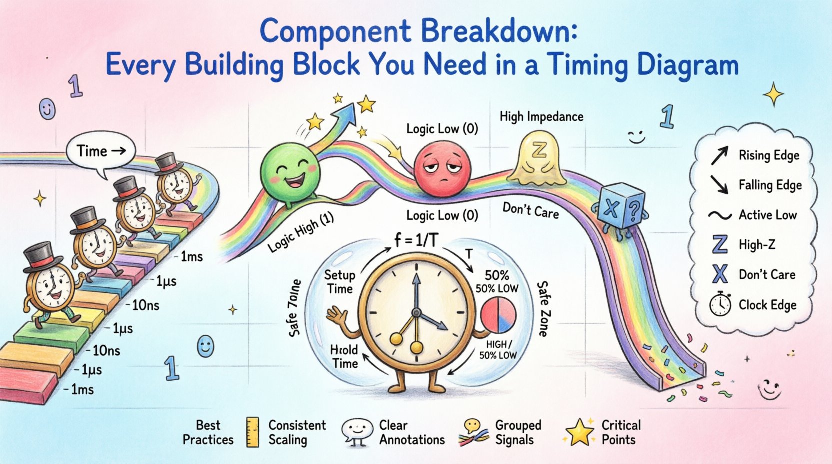
1. The Foundation: Axes and Time Scales ⏱️
Every timing diagram begins with a coordinate system. Without a defined time scale, the diagram is merely a qualitative sketch rather than a quantitative tool.
- Horizontal Axis (Time): This represents the progression of time. It typically flows from left to right. Units can vary based on the context, including seconds, milliseconds, microseconds, nanoseconds, or clock cycles.
- Vertical Axis (Signal Level): This represents the state of the signal. It is usually binary, showing High (1) or Low (0), but can also include analog voltage levels or multi-state logic values.
When setting up the horizontal axis, consistency is key. If you use a scale of 10 nanoseconds per grid line, all signals must adhere to this scale. This allows for accurate measurement of delays and periods between events.
2. Signal Lines and Identification 🔌
Each horizontal line in a timing diagram represents a specific signal. These lines are the primary carriers of information within the system.
Signal Naming Conventions
- Descriptive Names: Use names that describe function, such as Address Bus, Data Valid, or Clock Enable.
- Active Low Indicators: Signals that are active when low are often denoted with a bar over the name (e.g., Chip Select or nCS) or an active-low symbol.
- Bus Grouping: Multiple signals representing a bus (like Data 0-7) are often grouped together with a bracket or a slash to indicate width.
Signal Traces
The trace is the line connecting the points on the graph. The shape of the trace indicates the behavior of the signal.
- Constant Lines: A flat line indicates a steady state. If it stays high, the signal is permanently asserted. If it stays low, it is deasserted.
- Stepped Lines: Vertical transitions between levels represent changes in state. These should be drawn as straight vertical lines to imply instant switching in an ideal model, though real-world physics introduces transition time.
- Zigzag Lines: These often represent noise, glitches, or high-frequency oscillations that might occur during unstable transitions.
3. Signal States and Logic Levels 🟢🔴
Understanding the logic levels represented on the vertical axis is critical for correct interpretation.
Binary States
- Logic High (1): Typically represented by the upper position on the vertical axis. In TTL logic, this is often 5V. In CMOS, it is close to the supply voltage.
- Logic Low (0): Typically represented by the lower position on the vertical axis. This is usually 0V or ground.
Special States
- High Impedance (Z): Also known as Hi-Z. This state disconnects the signal from the driver, allowing other devices on the bus to control the line. It is often represented by a dashed line or a specific “Z” label.
- Don’t Care (X): Indicates that the value of the signal does not affect the outcome of the operation. It is often represented by an “X” symbol.
- Unknown (U): Used when the initial state is undefined at the start of a simulation.
4. Transitions and Edges 📉📈
Transitions are the moments where a signal changes state. These are the most critical parts of a timing diagram for clocking and data integrity.
Rising Edge
A rising edge occurs when a signal transitions from Low to High. In digital logic, this is often the trigger for positive-edge triggered flip-flops. It is visually represented by a vertical line moving upwards.
Falling Edge
A falling edge occurs when a signal transitions from High to Low. Negative-edge triggered devices respond to this transition. It is visually represented by a vertical line moving downwards.
Transition Time
While ideal diagrams show instant vertical lines, real signals have a finite transition time. This is the period required for the voltage to move from one logic threshold to another. In high-speed designs, this time is crucial because it determines how much bandwidth the signal consumes.
5. Clocking Mechanisms ⚙️
Clocks synchronize operations. Without a clock, asynchronous systems rely on handshakes, but most modern systems use a clock signal to define the rhythm of data processing.
Clock Period and Frequency
- Period (T): The time it takes for one complete cycle of the clock signal (from rising edge to the next rising edge).
- Frequency (f): The number of cycles per second, measured in Hertz (Hz). Frequency is the inverse of the period (f = 1/T).
Duty Cycle
The duty cycle is the percentage of one period in which the signal is high. A 50% duty cycle means the signal is high for half the period and low for the other half. Deviations from 50% can affect the timing of specific logic gates.
Phase Alignment
In multi-clock systems, the phase relationship between clocks matters. Two clocks might run at the same frequency but start at different points in their cycle. This is critical for systems with multiple clock domains.
6. Timing Constraints and Delays ⏳
Timing constraints define the acceptable window for signals to change. Violating these constraints leads to functional errors.
Setup Time
Setup time is the minimum amount of time before a clock edge that a data signal must be stable. If the data changes too close to the clock edge, the receiving device may not capture it correctly.
- Requirement: Data must be stable for X nanoseconds before the rising edge.
- Consequence of Violation: Metastability or incorrect data capture.
Hold Time
Hold time is the minimum amount of time after a clock edge that the data signal must remain stable. This ensures the data is latched securely.
- Requirement: Data must not change for Y nanoseconds after the rising edge.
- Consequence of Violation: Data corruption or race conditions.
Propagation Delay
This is the time it takes for a signal to travel from the input of a component to its output. It varies based on the physical path and the type of gate used.
Skew
Sky occurs when the same clock signal arrives at different components at different times. This can happen due to trace length differences on a circuit board. Skew reduces the effective setup and hold time margins.
7. Data Encoding and Validity 📝
Timing diagrams often show when data is valid relative to the clock or control signals.
Data Valid Window
There is a specific window during which the data on the bus is guaranteed to be correct. This is usually between the clock edge and the next edge, or between control signal assertions.
Encoding Schemes
- NRZ (Non-Return-to-Zero): Data is represented by the level of the signal. Simple but lacks a clock within the data stream.
- Manchester Encoding: Each bit is represented by a transition in the middle of the bit period. This ensures clock recovery is possible.
- 4B/5B: A block coding scheme used to ensure sufficient transitions for clock recovery while maintaining efficiency.
8. Types of Timing Diagrams 📑
Different contexts require different styles of timing diagrams.
Synchronous Timing Diagrams
These rely heavily on a master clock. All events are referenced to the clock edges. This makes analysis easier as timing is predictable and periodic.
Asynchronous Timing Diagrams
These do not rely on a global clock. Events are triggered by the completion of previous events (handshaking). The time between events is variable and depends on processing speed or network latency.
Protocol Timing Diagrams
These focus on the communication rules between two devices, such as I2C, SPI, or UART. They define start bits, stop bits, data bits, and acknowledgment signals.
9. Summary of Common Symbols 📋
The following table summarizes the standard symbols used in timing diagrams to improve readability and consistency.
| Symbol | Meaning | Usage Context |
|---|---|---|
| ↗ | Rising Edge | Positive edge triggered logic |
| ↘ | Falling Edge | Negative edge triggered logic |
| ___ | Logic Low (0) | Ground or inactive state |
| ___ | Logic High (1) | VCC or active state |
| ~ | Active Low | Signal is active when low |
| X | Don’t Care | Value does not impact logic |
| Z | High Impedance | Bidirectional bus floating |
| ⇨ | Propagation Delay | Time between input change and output change |
| ⏰ | Clock Edge | Synchronization point |
10. Best Practices for Documentation 📝
Creating a timing diagram that others can understand requires adherence to standards. Poor documentation leads to engineering errors.
- Consistent Scaling: Ensure the time scale is linear. Do not compress time in one section and expand it in another without clear indication.
- Clear Annotations: Add text notes to explain complex interactions. A diagram can become cluttered if it relies solely on lines.
- Group Related Signals: Place signals that interact closely together vertically. This reduces the eye travel required to understand the relationship.
- Mark Critical Points: Highlight setup and hold times explicitly. Use brackets or shaded regions to indicate valid windows.
- Version Control: If the design changes, update the diagram immediately. Outdated timing diagrams are worse than no diagram at all.
11. Common Pitfalls and Misinterpretations ⚠️
Even experienced engineers can misread timing diagrams. Being aware of common errors helps in verification.
Ambiguous Transitions
Some diagrams draw transitions that are not vertical. If a line is slanted, it implies a transition time. If it is vertical, it implies instant change. Be clear about which model you are using.
Missing Context
A diagram showing a signal going high is useless without knowing what triggers it. Always include the control signals that cause the data signal to change.
Scale Confusion
A common mistake is assuming a uniform scale across multiple diagrams. If Diagram A uses microseconds and Diagram B uses clock cycles, do not compare them directly without conversion.
Ignoring Glitches
Short pulses (glitches) are often omitted for clarity. However, in high-speed circuits, these glitches can trigger false states. Always note if glitches are filtered or ignored.
12. Practical Application in Debugging 🔍
Timing diagrams are the primary tool for debugging synchronization issues. When a system fails, the diagram helps isolate where the timing constraint was violated.
Step-by-Step Debugging
- Identify the Clock: Determine the reference clock for the failing subsystem.
- Check Data Stability: Verify that data lines are stable during the setup and hold windows relative to the clock edge.
- Measure Delays: Use an oscilloscope to measure actual propagation delays and compare them against the diagram specifications.
- Analyze Skew: Check if the clock signal is arriving at different times at different chips.
- Review Control Signals: Ensure enable signals are asserted correctly before data transfer begins.
13. Future Considerations in High-Speed Design 🚀
As technology advances, the requirements for timing diagrams become more stringent.
- Jitter: In very high frequencies, the clock edge itself may wander. Timing diagrams must account for jitter margins.
- Power Management: Dynamic voltage and frequency scaling (DVFS) can change timing parameters on the fly. Diagrams must reflect operating modes.
- Multi-Domain Systems: Modern chips integrate analog, digital, and RF sections. Timing diagrams must show how these domains interface.
14. Integrating with Other Documentation 📚
A timing diagram does not stand alone. It works best when integrated with other technical documents.
- Schematics: Show the physical connections that create the timing paths.
- State Machines: Show the logical flow that drives the timing signals.
- Register Maps: Show the configuration that determines timing behavior.
15. Final Thoughts on Signal Integrity 🛡️
Understanding the components of a timing diagram is essential for signal integrity. It bridges the gap between abstract logic and physical reality. By mastering the elements of time, state, and edge, engineers can design systems that are robust and reliable.
Remember that a timing diagram is a contract between the hardware and the software. It defines the rules of engagement. If the hardware does not follow the timing rules, the software cannot function correctly. Therefore, precision in these diagrams is not just a preference; it is a requirement.
Whether you are analyzing a simple LED blink or a complex multi-gigabit data stream, the components remain the same. Focus on the edges, respect the delays, and maintain clarity in your documentation. This approach ensures that your designs are clear, verifiable, and successful.